

TI TDA4VM的汽车电子程序应用案例
应用案例
描述
TI公司的TDA4VM处理器系列是基于Jacinto™ 7架构,目标用在驾驶辅助系统(ADAS)和无人驾驶汽车(AV).具有强大的片上数据分析的能力,并与视觉预处理加速器相结合,从而使得系统性能更高效.汽车厂商和一级供应商可用来开发前置摄像头应用,使用高分辨率的800万像素摄像头.帮助车辆看得更远并且可以加入更多驾驶辅助增强功能.此外,TDA4VM处理器能够同时操作4到6个300万像素的摄像头,同时还可以将雷达,激光雷达和超声波等其他多种感知处理融合在一个芯片上.这种多级处理能力使得tda4vm能够胜任ADAS的中心化处理单元,进而实现自动泊车应用中的关键功能(如环绕视图和图像渲染显示),同时增强车辆感知能力,实现360度的识别感知.TDA4VM处理器核采用C7x浮点,矢量DSP,高达1.0 GHz, 80 GFLOPS, 256 GOPS;深度学习矩阵乘法加速器(MMA),1.0GHz高达8 TOPS (8b);视觉处理加速器(VPAC)和图像信号处理器(ISP)和多个视角辅助加速器;深度和运动处理加速器(DMPAC);具有两个64位 Arm® Cortex®-A72微处理器子系统,工作频率高达1.8GHz,22K DMIPS;每个Cortex®-A72核集成了32KB L1 DCache和48KB L1 ICache,有六个Arm® Cortex®-R5F MCU,工作频率高达1.0GHz,12 K DMIPS;每个核存储器为64K L2 RAM,隔离MCU子系统有两个Arm® Cortex®-R5F MCU,通用计算部分有四个Arm® Cortex®-R5F MCU,两个C66x浮点DSP,工作频率高达1.35 GHz, 40 GFLOPS, 160 GOPS;TDA4VM处理器仅使用5到20W的功率执行高性能ADAS运算,无需主动冷却.TDA4VM是一个完全可编程的处理器.主要用在驾驶辅助系统(ADAS)和无人驾驶汽车(AV).本文介绍了TDA4VM主要特性,功能框图以及Jacinto7 J721E/DRA829/TDA4VM评估模块(EVM)主要特性,功能框图,EVM系统架构接口图,时钟架构图,功率分布框图,加电顺序图等以及电路图,材料清单,PCB设计图.
The TDA4VM processor family is based on the evolutionary Jacinto™ 7 architecture, targeted at ADAS and Autonomous Vehicle (AV) applications and built on extensive market knowledge accumulated over a decade of TI’s leadership in the ADAS processor market. The TDA4VM provides high performance compute for both traditional and deep learning algorithms at industry leading power/performance ratios with a high level of system integration to enable scalability and lower costs for advanced automotive platforms supporting multiple sensor modalities in centralized ECUs or stand-alone sensors. Key cores include next generation DSP with scalar and vector cores, dedicated deep learning and traditional algorithm accelerators, latest Arm and GPU processors for general compute, an integrated next generation imaging subsystem (ISP), video codec, Ethernet hub and isolated MCU island. All protected by automotive grade safety and security hardware accelerators.
Key Performance Cores Overview
The “C7x” next generation DSP combines TI’s industry leading DSP and EVE cores into a single higher performance core and adds floating point vector calculation capabilities, enabling backward compatibility for legacy code while simplifying software programming. The new “MMA” deep learning accelerator enables performance up to 8 TOPS within the lowest power envelope in the industry when operating at the typical automotive worst case junction temperature of 125°C. The dedicated ADAS/AV hardware accelerators provide vision pre-processing plus distance and motion processing with no impact on system performance.
General Compute Cores and Integration Overview
Separate dual core cluster configuration of Arm® Cortex®-A72 facilitates multi-OS applications with minimal need for a software hypervisor. Up to 4 Arm® Cortex®-R5F subsystems enable low-level, timing critical processing tasks to leave the Arm® Cortex®-A72’s unencumbered for applications. The integrated “8XE GE8430” GPU offers up to 100 GFLOPS to enable dynamic 3D rendering for enhanced viewing applications. Building on the existing world-class ISP, TI’s 7th generation ISP includes flexibility to process a broader sensor suite, support for higher bit depth, and features targeting analytics applications.
Integrated diagnostics and safety features support operations up to ASIL-D levels while the integrated security features protect data against modern day attacks. To enable systems requiring heavy data bandwidth, a PCIe hub and Gigabit Ethernet switch are included along with CSI-2 ports to support throughput for many sensor inputs. To further the integration, the TDA4VM family also includes an MCU island eliminating the need for an external system microcontroller.
TDA4VM主要特性:
1Processor cores:
• C7x floating point, vector DSP, up to 1.0 GHz, 80 GFLOPS, 256 GOPS
• Deep-learning matrix multiply accelerator (MMA), up to 8 TOPS (8b) at 1.0 GHz
• Vision Processing Accelerators (VPAC) with Image Signal Processor (ISP) and multiple vision assist accelerators
• Depth and Motion Processing Accelerators (DMPAC)
• Dual 64-bit Arm® Cortex®-A72 microprocessor subsystem at up to 1.8 GHz, 22K DMIPS
– 1MB shared L2 cache per dual-core Cortex®-A72 cluster
– 32KB L1 DCache and 48KB L1 ICache per Cortex®-A72 core
• Six Arm® Cortex®-R5F MCUs at up to 1.0 GHz, 12K DMIPS
– 64K L2 RAM per core memory
– Two Arm® Cortex®-R5F MCUs in isolated MCU subsystem
– Four Arm® Cortex®-R5F MCUs in general compute partition
• Two C66x floating point DSP, up to 1.35 GHz, 40 GFLOPS, 160 GOPS
• 3D GPU PowerVR® Rogue 8XE GE8430, up to 750 MHz, 96 GFLOPS, 6 Gpix/sec
• Custom-designed interconnect fabric supporting near max processing entitlement
Memory subsystem:
• Up to 8MB of on-chip L3 RAM with ECC and coherency
– ECC error protection
– Shared coherent cache
– Supports internal DMA engine
• External Memory Interface (EMIF) module with ECC
– Supports LPDDR4 memory types
– Supports speeds up to 3733 MT/s
– 32-bit data bus with inline ECC up to 14.9GB/s
• General-Purpose Memory Controller (GPMC)
• 512KB on-chip SRAM in MAIN domain, protected by ECC
Safety: targeted to meet ASIL-D for MCU island and ASIL-B for main processor
• Integrated MCU island subsystem of Dual Arm® Cortex®-R5F cores with floating point coprocessor and optional lockstep operation, targeted to meet ASIL-D safety requirements/certification
– 512B Scratchpad RAM memory
– Up to 1MB on-chip RAM with ECC dedicated for R5F
– Integrated Cortex®-R5F MCU island isolated on separate voltage and clock domains
– Dedicated memory and interfaces capable of being isolated from the larger SoC
• The TDA4VM main processor is targeted to meet ASIL-B safety requirements/certification
– Widespread ECC protection of on-chip memory and interconnect
– Built-in self-test (BIST) and fault-injection for CPU and on-chip RAM
– Error Signaling Module (ESM) with error pin
– Runtime safety diagnostics, voltage, temperature, and clock monitoring, windowed
watchdog timers, CRC engine for memory integrity checks
– Safety documentation available for applications required to meet ISO 26262 requirements
Device security:
• Secure boot with secure runtime support
• Customer programmable root key, up to RSA-4K or ECC-512
• Embedded hardware security module
• Crypto hardware accelerators – PKA with ECC, AES, SHA, RNG, DES and 3DES
High speed serial interfaces:
• Integrated ethernet switch supporting (total of 8 external ports)
– Up to eight 2.5Gb SGMII
– Up to eight RMII (10/100) or RGMII (10/100/1000)
– Up to two QSGMII
• Up to four PCI-Express® (PCIe) Gen3 controllers
– Up to two lanes per controller
– Gen1 (2.5GT/s), Gen2 (5.0GT/s), and Gen3 (8.0GT/s) operation with auto-negotiation
• Two USB 3.0 dual-role device (DRD) subsystem
– Two enhanced SuperSpeed Gen1 Ports
– Each port supports Type-C switching
– Each port independently configurable as USB host, USB peripheral, or USB DRD
Automotive interfaces:
• Sixteen Modular Controller Area Network (MCAN) modules with full CAN-FD support
Capture subsystem:
• Two CSI2.0 4L RX plus One CSI2.0 4L TX
– 2.5Gbps RX throughput per lane (20Gbps total) Display subsystem:
• One eDP/DP interface with Multi-Display Support (MST)
– HDCP1.4/HDCP2.2 high-bandwidth digital content protection
• One DSI TX (up to 2.5K)
• Up to two DPI
Audio interfaces:
• Twelve Multichannel Audio Serial Port (MCASP) Modules
Video acceleration:
• Ultra-HD video, one (3840 × 2160p, 60 fps), or two (3840 × 2160p, 30 fps) H.264/H.265 decode
• Full-HD video, four (1920 × 1080p, 60 fps), or eight (1920 × 1080p, 30 fps) H.264/H.265 decode
• Full-HD video, one (1920 × 1080p, 60 fps), or up to three (1920 × 1080p, 30 fps) H.264 encode
Flash memory interfaces:
• Embedded MultiMediaCard Interface ( eMMC™ 5.1)
• Universal Flash Storage (UFS 2.1) interface with two lanes
• Two Secure Digital® 3.0/Secure Digital Input Output 3.0 interfaces (SD3.0/SDIO3.0)
• Two simultaneous flash interfaces configured as
– One OSPI and one QSPI flash interfaces
– or HyperBus™ and QSPI flash interface
System-on-Chip (SoC) architecture:
• 16-nm FinFET technology
• 24 mm × 24 mm, 0.8-mm pitch, 827-pin FCBGA (ALF), enables IPC class 3 PCB routing
TPS6594-Q1 Companion Power Management
ICs (PMIC):
• Functional Safety support up to ASIL-D
• Flexible mapping to support different use cases
TDA4VM应用:
• Advanced surround view and park assistance systems
• Autonomous sensor fusion / perception systems including camera, radar and lidar sensors
• Mono and multi-sensor Front camera systems
• Next generation eMirror systems
图1.TDA4VM功能框图
Jacinto7 J721E/DRA829/TDA4VM评估模块(EVM)
The Jacinto7 J721E (DRA829/TDA4xM) EVM is a standalone test, development, and evaluation module system that enables developers to write software and develop hardware around Jacinto7 J721E (DRA829/TDA4xM) processor subsystem. The J721E processor is a KeyStone™ III-based Multicore Arm® System-on-Chip (SoC). It is a super-set processor/device and may be available is different configurations targeted for specific markets. This EVM will support development of the super-set device (J721E) as well as the market specific devices (DRA829/TDA4xM). Many features of the J721E system are available on the EVM, which gives developers the basic resources needed for most general-purpose type.
The J721E EVM is comprised of:
• J721E System On Module (SOM) board
• Jacinto7 Common Processor Board (CPB)
• Quad-Port Ethernet board (QPENet)
J721E EVM sub system has been designed to enable customers to evaluate the Processor’s performance with flexibility. To have flexibility while developing the system, different interface/expansion boards have been designed. Some examples include:
• Infotainment Expansion Board
• Gateway/Ethernet Switch/Industrial (GESI) Expansion Board
• Fusion CSI2 Expansion Board(s)
Jacinto7 J721E/DRA829/TDA4VM评估模块(EVM)主要特性:
The J721E EVM is a high performance, standalone development platform that enables users to evaluate the Texas Instrument’s Keystone III System-on-Chip (SoC).
Below are the EVM’s key features:
• Processor:
– J721E (DRA829/TDA4xM), 24 mm x 24 mm, 0.8 mm pitch, 827-pin FCBGA
– Support for corresponding socket
• Power Supply:
– 12 V DC nominal input (6 V-28 V input range)
– Optimized Power Management Solution for Processor
– Integrated Power Measurement
• Memory:
– DRAM, LPDDR4-3733, 4GByte total memory, support inline ECC
– 2x Octal-SPI NOR flash, 512 Mb memory (8 bit) + 512 Mb memory (4 bit)
– HyperFlash + HyerRAM, 512 Mb flash memory + 256 Mb RAM
– UFS Flash memory, 32GByte, 2Lane, Gear3
– eMMC Flash memory, 16 GB memory, v5.1 compliant
– MicroSD Card Cage, UHS-I
– Inter-Integrated Circuit (I2C) EEPROM, 1 Mbit
• JTAG/Emulator:
– Integrated XDS110 Emulator support
– External emulator through 60pin MIPI Connector
– Trace Support through 60pin MIPI Connector
– Includes adapters for 14pin and 20pin CTI
• Supported Interfaces and Peripherals:
– 4x CAN Interfaces, full CAN-FD support
– 1x USB3.1 Type C Interface, support DFP, DRP, UFP modes
– 4x USB2.0 Host Interfaces (2x for external cables)
– 1x Display Port, up to 4K resolution with MST support
– 1x FPD-Link Panel Interface, Gen3
– 1x Audio Codec (PCM3168A), supports 2x Line Inputs, 4x Microphone Inputs, 2x Line Outputs, 6x Headphone Outputs
– 1x FPD-Link Radio Tuner Interface
– 2x PCIe Card Slot, 1x PCIe M.2 Slot (M-Key), all Gen3
– 5x Gbit Ethernet, 1x RGMII/DP83867 + 1x QSGMII/VSC8514
– 6x Universal Asynchronous Receiver/Transmitter (UART) terminals via 2x USB FTDI (UART-over-USB)
– 2x I3C headers
– 1x ADC Header
• Expansion Connectors to support application specific add-on boards
– MLB, MLBP Expansion Interface
– Image/Video Capture Expansion Interface
– Apple Authentication Module Interface
– General Expansion Interface
• REACH and RoHS Compliant
图2.J721E/DRA829/TDA4VM评估模块EVM外形图
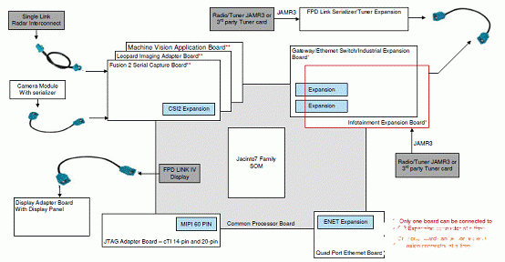
图3.J721E/DRA829/TDA4VM评估模块EVM系统架构接口图
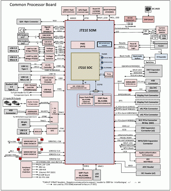
图3.J721E/DRA829/TDA4VM评估模块EVM功能框图
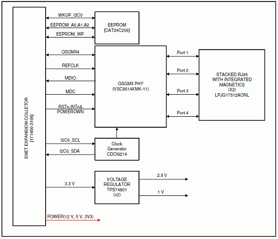
图4.四端口以太网扩展功能框图
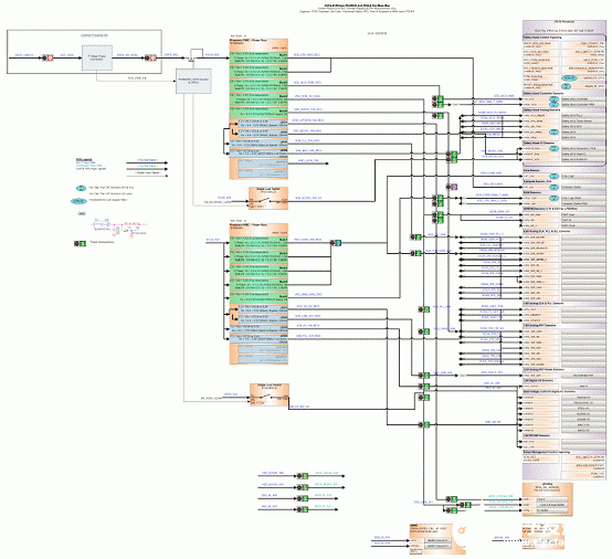
图5.J721E SOM功率分布框图
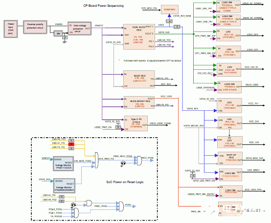
图6.加电顺序图
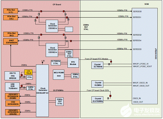
图7.EVM时钟架构图
The TDA4VMXEVM is an eva
luation platform designed to speed up development efforts and reduce time to market for ADAS applications.
The TDA4x EVM is based on a TDA4VMx System-on-Chip (SoC) that incorporates a powerful heterogeneous, scalable architecture that includes a mix of TI’s fixed and floating-point TMS320C66x Digital Signal Processor (DSP) cores, the C71x DSP Core and Matrix Math Accelerator for AI, Arm® Cortex®-A72 cores, integrated ISP and vision processing acceleration, 2D and 3D GPU cores, H.264 encode/H.265 decode acceleration. An on-chip Safety island featuring dual-lockstep R5F cores helps the system achieve ASIL-D level certification while reducing the need for an external safety microcontroller, further reducing system bill-of-materials. On-chip peripherals allow for multi-camera input via CSI-2 ports, vehicle connectivity based on PCI Express, CAN-FD and Gigabit Ethernet, and display connectivity via DSI interfaces.
The EVM is supported by the Processor SDK-Vision which includes foundational drivers, compute and vision kernels, and example application frameworks and demonstrations that show users how to take advantage of the powerful heterogeneous SoC architecture.
-
基于双TDA4VM行泊一体方案2022-11-03 0
-
TDA4对深度学习的重要性2022-11-03 0
-
TI中DSP应用开发实用子程序2018-04-10 482
-
TDA4VM 处理器可以满足现代车辆的计算需求2020-08-12 22823
-
带参数子程序的参数传递过程2022-10-17 1963
-
双TDA4VM NOA行泊一体化解决方案2022-11-04 1853
-
基于TI AWR2944和TDA4VM的汽车级安全OS2022-12-27 806
-
将现有的Jetson Nano项目移植到TI SK-TDA4VM2023-06-12 375
-
开始使用TI SK-TDA4VM开发套件2023-07-13 389
-
面向TI TDA4VM处理器的恩智浦PMIC解决方案2023-08-17 128
-
一文详解PLC子程序与子程序指令2023-12-14 3113
全部0条评论

快来发表一下你的评论吧 !
