

P-FET Linear Regulator Has Low
电源设计应用
419人已加入
描述
P-channel MOSFETs (P-FETs), though more expensive than pnp transistors, are free of the dissipation loss associated with base drive in a pnp circuit. P-FETs also have a lower saturation voltage at light loads (Figure 1). In fact, the low rDS(ON), logic-level, p-channel power MOSFETs currently available can regulate 5V from a 5.1V battery!
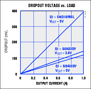
Figure 1. A p-channel MOSFET (Q1) allows this linear regulator to operate with VIN to-VOUT differentials lower than 100mV.
This capability lets the Figure 2 circuit derive 5V ±10% from four battery cells, even when they've discharged as low as 4.6V. Low dropout voltage lets the circuit "ride down" on the declining battery voltage, finally falling out of regulation at approximately 4.6V. The low input-to-output differential at that time (0.1V) allows nearly 100% efficiency. Note that the output accuracy of IC1 (±0.6% over temperature) makes it suitable as a 2.5V system reference.
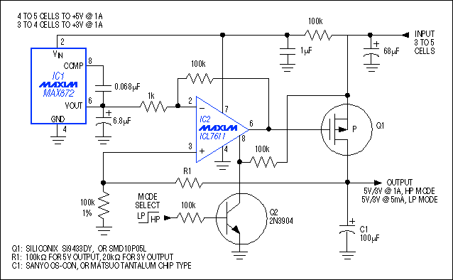
Figure 2. At low output current, these p-channel MOSFETs exhibit low source-to-drain voltage (i.e., dropout voltage in the Figure 1 circuit).
IC2's pin-programmable bias current makes possible a low-power mode in which the entire circuit draws less than 50µA. Five milliamps is available in this mode for circuitry such as backup RAM and a real-time clock. In high-power mode, the regulator can deliver 1A.
The 100µF output capacitor (C1) is chosen to accomodate the maximum load currents of 1A; for lighter loads you can scale the capacitor to a smaller value. Beware, though-the circuit's loop stability depends on lag compensation in which 1/2πRESRC1 > 14kHz, where RESR is C1's equivalent series resistance. (Figure 1 recommends acceptable capacitor types for C1.)
Configured for a 5V output (R1 = 100kΩ), the circuit can deliver 500mA from five cells producing 7.5V, or 1A from four cells producing 6V. Configured for 3V (R1 = 20kΩ), it delivers 500mA from four cells producing 6V, or 1A from three cells producing 4.5V. The input voltage can range from 3V to 15V, subject to a limitation; with no heatsink on Q1, the MOSFET's package-dissipation rating limits the input voltage and output current as follows: IOUT × (VIN VOUT) < 1.25W.
打开APP阅读更多精彩内容
Figure 1. A p-channel MOSFET (Q1) allows this linear regulator to operate with VIN to-VOUT differentials lower than 100mV.
This capability lets the Figure 2 circuit derive 5V ±10% from four battery cells, even when they've discharged as low as 4.6V. Low dropout voltage lets the circuit "ride down" on the declining battery voltage, finally falling out of regulation at approximately 4.6V. The low input-to-output differential at that time (0.1V) allows nearly 100% efficiency. Note that the output accuracy of IC1 (±0.6% over temperature) makes it suitable as a 2.5V system reference.
Figure 2. At low output current, these p-channel MOSFETs exhibit low source-to-drain voltage (i.e., dropout voltage in the Figure 1 circuit).
IC2's pin-programmable bias current makes possible a low-power mode in which the entire circuit draws less than 50µA. Five milliamps is available in this mode for circuitry such as backup RAM and a real-time clock. In high-power mode, the regulator can deliver 1A.
The 100µF output capacitor (C1) is chosen to accomodate the maximum load currents of 1A; for lighter loads you can scale the capacitor to a smaller value. Beware, though-the circuit's loop stability depends on lag compensation in which 1/2πRESRC1 > 14kHz, where RESR is C1's equivalent series resistance. (Figure 1 recommends acceptable capacitor types for C1.)
Configured for a 5V output (R1 = 100kΩ), the circuit can deliver 500mA from five cells producing 7.5V, or 1A from four cells producing 6V. Configured for 3V (R1 = 20kΩ), it delivers 500mA from four cells producing 6V, or 1A from three cells producing 4.5V. The input voltage can range from 3V to 15V, subject to a limitation; with no heatsink on Q1, the MOSFET's package-dissipation rating limits the input voltage and output current as follows: IOUT × (VIN VOUT) < 1.25W.
声明:本文内容及配图由入驻作者撰写或者入驻合作网站授权转载。文章观点仅代表作者本人,不代表电子发烧友网立场。文章及其配图仅供工程师学习之用,如有内容侵权或者其他违规问题,请联系本站处理。
举报投诉
- 相关推荐
- Voltage
-
12V,500mA linear regulator circuit2011-01-08 0
-
如何用PNP管更换P-FET?2017-11-20 0
-
AMC7635,pdf datasheet (LOW DRO2009-08-27 426
-
LFC789D25,PDF(DUAL LINEAR FET2010-10-22 563
-
CISSOID推出高温30V小讯号P-FET场效应管2010-12-20 1076
-
MAX15101,Low-Dropout Linear Regulator2012-01-17 659
-
pFET Linear Regulator Has Low Dropout Voltage2017-04-10 418
-
LT3072 Demo Circuit - Dual 2.5A, Low Noise, Programmable Output, 80mV Dropout Linear Regulator (0.8-3.45V to 0.6-2.5V @ 2.5A x 2)2021-01-28 428
-
LT3072: Dual, Low Noise, 2.5A Programmable Output, 80mV Low Dropout Linear Regulator Datasheet2021-01-28 532
-
LT3070-1 Demo Circuit - Low Voltage, UltraFast™ Transient Response Linear Regulator (1.2V to .9V @ 5A)2021-02-01 433
-
LT3010 Demo Circuit - µPower Linear Regulator (2.2-30V to 1.8V @ 50mA)2021-02-03 420
-
LT3045 Demo Circuit - Low Noise, High PSRR RF Linear Regulator (3.8-20V to 3.3V @ 500mA)2021-02-20 573
-
MAX25210: Automotive Ultra Low Quiescent Current Linear Regulator Family Data Sheet MAX25210: Automotive Ultra Low Quiescent Current Linear2023-10-13 19
全部0条评论

快来发表一下你的评论吧 !
