

Power Supply and Accurate Curr
新品快讯
描述
Power Supply and Accurate Current Monitor for Avalanche Photodiode (APD) Biasing Applications
Abstract: This reference design presents a circuit for addressing the power-supply and current-monitoring requirements of APD biasing applications. Based on the MAX15031 DC-DC converter, the application circuit provides a 70V, 4mA, DC-DC power converter with a 2.7V to 11V input supply-voltage range.
Key specifications for this reference design are listed below, along with a detailed schematic (Figure 1) and bill of materials (Table 1) for the application.
Design Specifications and Setup
- Wide, 2.7V to 11V input supply-voltage range
- 70V output voltage
- 4mA output current
- Fixed, 400kHz switching frequency
- -40°C to +125°C operating temperature range
- Tiny, 8mm x 12mm circuit footprint
Schematic of the Reference Design
Figure 1 presents the reference design schematic for a 2.7V to 5.5V input range. The same circuit can be used for inputs from 5.5V to 11V by connecting the CP pin to VIN and removing the charge-pump capacitor (C3).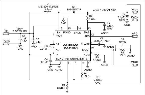
Figure 1. Schematic of the MAX15031 boost converter for FSW = 400kHz (fixed).
Table 1. Bill of Materials (BOM)
| Designator | Value | Description | Part | Footprint | Manufacturer | Quantity |
| C1 | 1µF, 10V | Capacitor | GRM155R61A105KE15 | 0402 | Murata | 1 |
| C2, C4 | 0.1µF, 16V | Capacitors | GRM155R71C104KA88 | 0402 | Murata | 2 |
| C3, C6 | 0.01µF, 25V | Capacitors | GRM155R71E103KA01D | 0402 | Murata | 2 |
| C5, C8 | 0.1µF, 100V | Capacitors | GCM21BR72A104KA37L | 0805 | Murata | 2 |
| C7 | 0 | Capacitor | Open | 0402 | Open | 1 |
| D1 | 100V, 150mA | Schottky diode | BAT46W-7-F | SOD-123 | Diodes Inc. | 1 |
| L1 | 4.7µH | Inductor | ME3220-472MLB | 3mm x 3mm | Coilcraft | 1 |
| R1 | 348kΩ | Resistor | SMD, 1%, 0.125W | 0402 | Vishay | 1 |
| R2 | 6.34kΩ | Resistor | SMD, 1%, 0.125W | 0402 | Vishay | 1 |
| R3, R6 | 10kΩ | Resistors | SMD, 1%, 0.125W | 0402 | Vishay | 2 |
| R4 | 100Ω | Resistor | SMD, 1%, 0.125W | 0402 | Vishay | 1 |
| R5 | 3.16kΩ | Resistor | SMD, 1%, 0.125W | 0402 | Vishay | 1 |
| U1 | MAX15031 | Boost converter | MAX15031ATE+ | 16-TQFN-EP | Maxim | 1 |
Waveforms Depicting the Performance of the Design
Figure 2 and Figure 3 show the performance of the Figure 1 circuit. From the LX node voltage, it can be known that the converter is operating in a discontinuous mode of operation. The circuit is designed for a 70V output (VOUT) while the input (VIN) is kept at 3.3V. 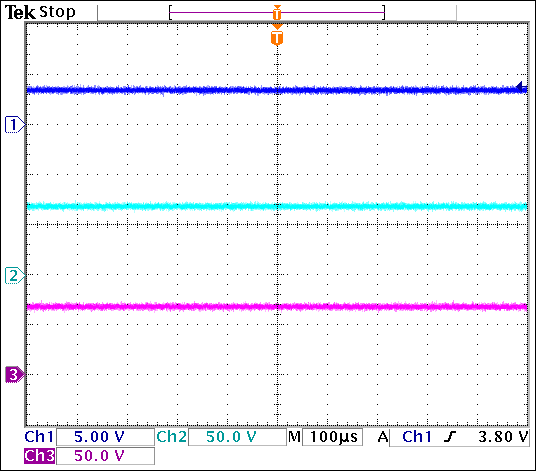
Figure 2. VIN (Channel 3), VOUT (Channel 2), and APD (Channel 1) at 3.3V input.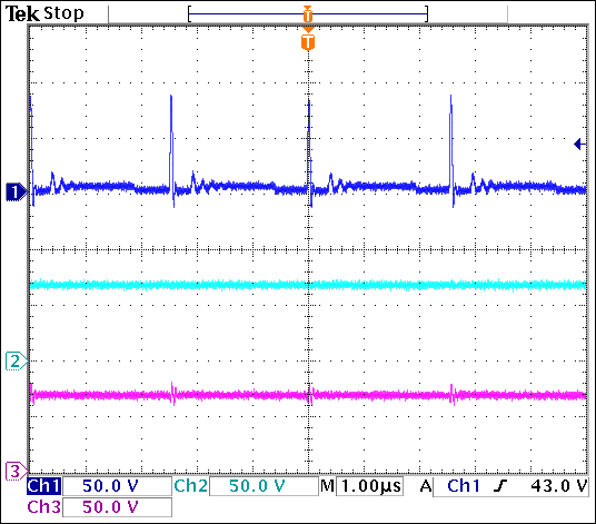
Figure 3. LX node voltage (Channel 1), VOUT (Channel 2), and APD output (Channel 3) at VIN =3.3 V with an APD current of 4mA.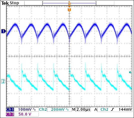
Figure 4. Input ripple (Channel 1) and output ripple (Channel 2) at VIN = 3.3V with an APD current of 4mA.
Figure 4 shows the input (VIN) and output (VOUT) ripple when input voltage is kept at 3.3V and the load current is 4mA.
Figure 5 shows the voltage across RLIM when the current reaches the current limit. In this case, the current limit is set at 4mA. When the current limit is reached, the voltage across RLIM is equal to 1.245V.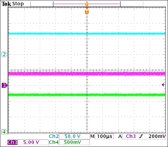
Figure 5. APD (Channel 2), VIN (Channel 3), and APD current-monitoring output across RLIM (Channel 4) at 4mA of APD current.
Efficiency Measurements
Efficiency of the total system is calculated from the test results with 3.3V and 5V inputs, and with the load current varied from 0 to 4mA. Figure 6 shows the efficiency curve for a 70V output.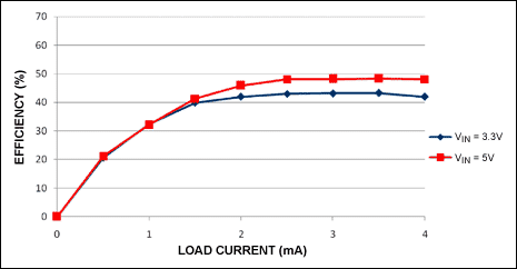
Figure 6. Efficiency versus load current with 3.3V and 5V inputs.
Board Design
Figure 7 shows the layout of this reference design, which fits on a tiny, 12mm x 8mm circuit board. Figure 8 and Figure 9 show the top-layer and bottom layer components, respectively.
Figure 7. Board layout of the reference design, which measures 12mm x 8mm.
Figure 8. Top-layer components.
Figure 9. Bottom-layer components.
- 相关推荐
- applicatio
-
Transformerless Power Supply 设计电路图2008-10-13 0
-
External-Sync Power Supply2009-03-27 0
-
switching power supply (SMPS)开关频率2009-04-08 0
-
HIGH CURRENT OFF LINE POWER SUPPLY2009-05-12 0
-
Power Supply and Ground Design for a WiFi Transceiver2011-01-28 0
-
SWITCH POWER SUPPLY DESIGN2012-08-16 0
-
power_supply框架包括哪些功能?2021-07-28 0
-
2W Non-isolated Power Supply u2009-06-28 813
-
Power Supply Management—Principles2009-09-25 419
-
Power Supply Cookbook2009-10-16 440
-
atx switching power supply2009-12-24 776
-
48W 2 Output Power Supply2010-01-07 520
-
Accurate Power Measurements on2010-03-03 425
-
W-CDMA Power Supply Dramatical2009-07-22 669
-
MAX16064 Quad power-supply con2009-10-31 847
全部0条评论

快来发表一下你的评论吧 !
