

Pipeline ADCs Come of Age
AD技术
描述
Pipeline ADCs Come of Age
Abstract: In the mid 1970s, a new data converter architecture was introduced to the analog and mixed-signal community, called pipeline ADCs. The following article takes the knowledge of advantages and disadvantages of the pipeline architecture and compares its features with four of the most popular architectures (flash, dual-slope, sigma-delta, and successive approximation) for analog-to-digital converters (ADCs). The paper concludes with an applications example for CCD imaging and discusses in detail why a pipeline-based ADC architecture is more desirable in such applications than any of the other commonly used concepts.
Since the mid-1970s, monolithic analog-to-digital converters (ADCs) have employed integrating, successive-approximation, and flash techniques. In the 1980s, delta-sigma designs further extended the range of choice. More recently, there has appeared a new class of ADC with an architecture known as "pipeline." Now offered by several manufacturers, pipeline ADCs offer an attractive combination of speed, resolution, low power consumption, and small die size (which equates to low cost). The features and benefits of this new architecture, however, are not yet widely understood.
The success of recent ADCs from several manufacturers—including Maxim—indicates that pipeline-architecture (or subranging) ADCs are among the most efficient and powerful data converters available. They offer high speed, high resolution, and excellent performance, along with modest levels of power dissipation and small die size. Within reasonable design limits they also offer excellent dynamic performance.
This article compares key characteristics of the five most popular techniques for analog-to-digital (A/D) conversion. Also included is an in-depth review of the operation, features, and benefits of pipeline architecture. The article concludes with a design example that features a pipeline ADC in a CCD imaging system.
Direct-conversion ADCs
Of the five techniques mentioned, one of the fastest is direct conversion, better known as "flash" conversion. ADCs based on this architecture are extremely fast and perform their multibit conversion directly, but they require intensive analog design to manage the large number of comparators and reference voltages required. As shown in Figure 1, a converter with N-bit resolution has 2N-1 comparators connected in parallel, with reference voltages set by a resistor network and spaced VFS/2N (~1 least significant bit, or LSB) apart.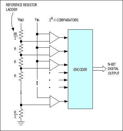
Figure 1. ADCs based on the direct-conversion architecture (better known as flash converters) include 2N-1 comparator banks and a reference resistor-divider network.
A change of input voltage usually causes a change of state in more than one comparator output. These output changes are combined in a decoder-logic unit that produces a parallel N-bit output from the converter. Although flash converters are the fastest types available (products like the future MAX104 offer sampling rates to 1GHz), their resolution is constrained by the available die size and by excessive input capacitance and power consumption caused by the large number of comparators used. Their repetitive structure demands precise matching between the parallel comparator sections, because any mismatch can cause static error such as a magnified input offset voltage (or current).
Flash ADCs are also prone to sporadic and erratic outputs known as "sparkle codes." Sparkle codes have two major sources:
- Metastability in the 2N-1 comparators
- Thermometer-code bubbles
Mismatched comparator delays can turn a logical 1 into 0 (or vice versa), causing the appearance of "bubbles" in an otherwise normal thermometer code. Because the ADC's encoder unit cannot detect this error, it generates an out-of-sequence code that also appears as an output "spark."
Another concern with flash ADCs is its die size, which is nearly seven times larger for an 8-bit flash converter than for the equivalent pipelined ADC. In further contrast to pipeline designs, the flash converter's input capacitance can be six times higher and its power dissipation twice as high.
Successive-approximation ADCs
The conversion technique based on a successive-approximation register (SAR), also known as bit-weighing conversion, employs a comparator to weigh the applied input voltage against the output of an N-bit digital-to-analog converter (DAC). Using the DAC output as a reference, this process approaches the final result as a sum of N weighting steps, in which each step is a single-bit conversion.
The first step stores the DAC's most significant bit (MSB) in the SAR, and the next step compares that value (the MSB) against the input. The comparator output (high or low) is fed to the DAC as a correction before the next comparison is made (Figure 2). Clocked by a logic control circuit, the SAR continues this weighing and shifting process until it completes the LSB step, which produces a DAC output within ±½LSB of the input voltage. As each bit is determined, it is latched into the SAR as part of the ADC's output.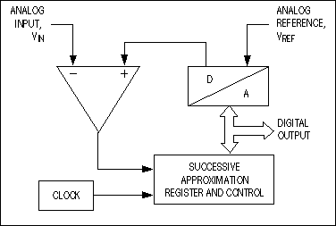
Figure 2. Typical successive-approximation ADCs consist of a single DAC, a comparator, and a successive-approximation register (SAR), plus a clock and logic control.
SAR converters consist of one comparator, one DAC, one SAR, and a logic control unit. They sample at rates to 1Msps, draw low supply current, and offer the lowest production cost, but their analog design is intensive and time consuming. Compared to a pipelined conversion structure, SAR ADCs provide a lower input bandwidth and sampling rates without latency problems.
Integrating ADCs
Integrating ADCs, also called dual- or multi-slope data converters, are among the most popular converter types. The classical dual-slope converter has two main sections: a circuit that acquires and digitizes the input, producing a time-domain interval or pulse sequence; and a counter that translates the result into a digital output value (Figure 3).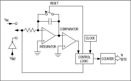
Figure 3. For slowly changing signals, one of the slowest but simplest conversion techniques employs an integrator that charges with the input voltage and discharges with an opposite-polarity reference voltage.
The dual-slope converter employs an analog integrator with switched inputs, a comparator, and a counter unit. The input voltage is integrated for a fixed time interval (TCHARGE) that usually corresponds to the maximum count of the internal counter unit (Figure 4). At the end of this interval the device resets its counter and applies an opposite-polarity (negative) reference to the integrator input. With this opposite-polarity signal applied, the integrator "deintegrates" until its output reaches zero, which stops the counter and resets the integrator.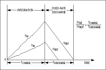
Figure 4. These voltage waveforms illustrate timing relationships for a dual-slope integrating ADC.
Charge gained by the integrator capacitor during the first, integrating/charging interval (TCHARGE/|VIN|) must equal that lost during the second, deintegrating/discharging interval (TDISCHARGE/|VREF|). Then the binary output is proportional to the ratio of these time intervals relative to the full count. TDISCHARGE at the end of the second interval corresponds to the ADC's output code. The relationship of VIN, VREF, TCHARGE, and TDISCHARGE is as follows:
The system can null any offsets during a conversion by initiating a calibration cycle within the converter. Compared to pipeline ADCs, the integrating types are extremely slow devices with low input bandwidths. But their ability to reject high-frequency noise and fixed low frequencies such as 50Hz or 60Hz makes them useful in noisy industrial environments and applications for which high update rates are not required (i.e., digitizing the outputs of strain gauges and thermocouples).
Sigma-delta (Σ-Δ ) ADCs
Sigma-delta (Σ-Δ ) converters have relatively simple structures. Also called oversampling converters, they consist of a Σ-Δ modulator followed by a digital decimation filter (Figure 5). The modulator, whose architecture is similar to that of a dual-slope ADC, includes an integrator and a comparator with a feedback loop that contains a 1-bit DAC. This internal DAC is simply a switch that connects the comparator input to a positive or negative reference voltage. The Σ-Δ ADC also includes a clock unit that provides proper timing for the modulator and digital filter.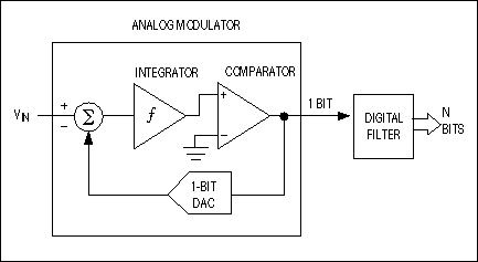
Figure 5. The two major building blocks of a sigma-delta converter are the analog modulator and the digital decimation filter.
Low-bandwidth signals applied to the input of a Σ-Δ ADC are quantized with very low (1-bit) resolution, but with a high sampling frequency of 2MHz or higher. Combined with digital post-filtering, this oversampling reduces the sampling rate to about 8kHz and increases the ADC's resolution (i.e., dynamic range) to 16 bits. Although slower than pipeline ADCs and limited to lower input bandwidths, the Σ-Δ principle has developed a strong position in the data-converter market. It offers three major advantages:
- Low-cost, high-performance conversion
- Digital filter included with the conversion circuitry
- DSP-compatible for system integration
What is a "pipeline" ADC?
Because pipeline ADCs provide an optimum balance of size, speed, resolution, power dissipation, and analog design effort, they have become increasingly attractive to major data-converter manufacturers and their designers. Also known as subranging quantizers, pipeline ADCs consist of numerous consecutive stages, each containing a track/hold (T/H), a low-resolution ADC and DAC, and a summing circuit that includes an interstage amplifier to provide gain.
Target applications for pipeline ADCs include communication systems, in which total harmonic distortion (THD), spurious-free dynamic range (SFDR), and other frequency-domain specifications are significant; CCD-based imaging systems, in which favorable time-domain specifications for noise, bandwidth, and fast transient response guarantee quick settling; and data-acquisition systems, in which time- and frequency-domain characteristics are both important (i.e., low spurs and high input bandwidth) are both important.
Fast and accurate N-bit conversions can be accomplished using at least two or more steps of subranging (also called pipelining). A coarse, M-bit A/D conversion is executed first (Figure 6). Then, using a DAC with at least N-bit accuracy, the result is converted back to one of 2M analog levels and compared with the input. Finally, the difference is converted with a "fine" K-bit flash converter and the two (or more) output stages are combined.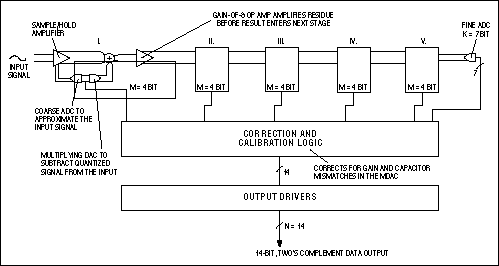
Figure 6. This simplified functional diagram shows the internal error correction and calibration logic for the MAX1200 family of 14-bit, 5-stage pipeline ADCs.
The following inequality should be met to correct for overlapping errors:
L × M+K > N
where L is the number of stages (depends on the manufacturer), M is the coarse resolution of subsequent stages in the ADC/MDAC circuit, K is the fine resolution of the final ADC stage, and N is the pipeline ADC's overall resolution. Most pipeline ADCs include digital error-correction circuitry that operates between the stages.
Some pipeline quantizers feature a calibration unit that compensates for unwanted side effects such as temperature drift or capacitor mismatch in the multiplying DAC. This digital calibration is usually performed for several (not all) of the pipeline's consecutive stages, using two adjacent codes that cause a transition equal to VREF at the MDAC output. Any deviation from this ideal step is an error that can be measured. When all errors have been acquired and accumulated by the subsequent converter stages, they are stored in an on-board memory. Then the results are fetched from RAM during normal operation to redeem gain and capacitor mismatches in the MDAC stages of the pipeline.
As an example, the calibration procedure for Maxim's family of 5-stage pipeline ADCs (MAX1200, MAX1201, and MAX1205) progresses from the pipeline's output to its inputs, just as described in the previous section. Only the first three stages are error-corrected. The third stage is corrected first (to improve linearity), and then the second stage is corrected. Those two error-corrected stages then enable calibration of the first stage.
The new pipeline architectures simplify ADC design and provide other advantages as well:
- Extra bits per stage optimize correction for overlapping errors.
- Separate track-and-hold (T/H) amplifiers for each stage release each previous T/H to process the next incoming sample, enabling conversion of multiple samples simultaneously in different stages of the pipeline.
- Lower power consumption.
- Higher-speed ADCs (fCONV > 100ns, typical) entail less cost and less design time and effort.
- Fewer comparators to become metastable virtually eliminates sparkle codes and thermometer bubbles.
But pipeline ADCs also impose difficulties:
- Complex reference circuitry and biasing schemes.
- Pipeline latency, caused by the number of stages through which the input signal must pass.
- Critical latch timing, needed for synchronization of all outputs.
- Sensitivity to process imperfections that cause nonlinearities in gain, offset, and other parameters.
- Greater sensitivity to board layout, compared with other architectures.
A multilayer board with properly designed layout can overcome some of these drawbacks. Also important is the selection of external components and the right choice of pipeline ADC—preferably one that includes onboard calibration of both gain and error mismatches (if any) between stages.
Design Example: Pipeline ADCs in CCD Imaging Applications
Imaging applications are proliferating, with an annual market growth in excess of 35%. Products include video cameras, camcorders, digital still-cameras, professional video, document scanners, and security systems. These applications employ two primary forms of the imaging sensor:
- CMOS imaging elements
- Charge-coupled devices (CCDs)
CMOS-based elements remove some of the constraints associated with CCDs, such as noise and temperature-coefficient considerations. Their pixels can be read one by one, but this reading frequency is limited to 30 frames per second and the output requires special design-intensive pixel processing.
CCDs are used in most of today's applications because they provide the best sensitivity and dynamic range. CCD resolution ranges from 1x256 to 512x512 pixels and even higher. To capture the incoming photons, each pixel consists of one "charge bucket" (three in an RGB CCD).
The CCD is the central element in an imaging system. All other circuitry simply supports the stringent and specific signal conditioning necessary to achieve maximum performance. Typical output signal levels for a CCD are very low, and they suffer from the detrimental effects of various noise sources. Designers must be aware of these characteristics and the special techniques necessary for dealing with them effectively.
In a typical CCD system (Figure 7), the CCD output is a serial stream of pixel "charges," shifted at high rates from the typical CCD format to one of stepped DC-voltage levels. This sequence of pulses rides on a DC bias (or offset voltage) of 10V or higher. For this reason, CCD outputs are capacitively coupled to the lower-voltage downstream signal-processing elements. Prior to pre-amplification and processing, a clamp or dc-restoration circuit is necessary to maintain the "dark baseline" level that corresponds to zero pixel charge.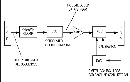
Figure 7. This simplified block diagram shows the major components of a typical CCD system.
Noise, the main restriction on sensitivity and dynamic range in a CCD application, must be carefully controlled. Noise sources include:
- kT/C noise, caused by FET switching resistance (RON) in the CCD output
- Circuit noise, 1/f noise, and shot noise
- Quantization noise (q/√12)
- 60Hz AC-line interference
- White or thermal noise caused by resistors and conductors in the circuitry: eWN = √4kTBROUT, where
k = 1.38054 10-23 (Boltzmann's constant)
where RL is the load resistor and RON represents the FET's on-resistance.
T = temperature in degrees Kelvin (298°K = +25°C)
B = noise bandwith (Hz)
ROUT = CCD output-stage resistance
(ROUT = RL + RON).
Processing the CCD output
The CCD output is not a continuous periodic waveform, but resembles a series of steps with different amplitudes or dc levels (Figure 8). In each cycle, pixel information is contained in the lower portion of the waveform. For circuit elements in the signal processing chain including the ADC, the characteristics of this waveform dictate that time- rather than frequency-domain specifications are the primary concern. Following the CCD element, a pre-amplifier boosts the signal level and a clamp restores the dc reference (black) level.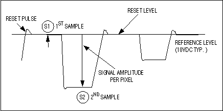
Figure 8. Each cycle of the CCD output signal contains pixel information in the lower portion of the waveform.
As mentioned earlier, the dominant kT/C noise is most significant in limiting the effective resolution in a CCD imaging system. To reduce this noise, the signal path should include a unit for correlated double-sampling (CDS). This name is taken from the double-sampling approach used to remove unwanted noise components: A sample (S1) is taken at the end of the reset period shown in Figure 3, and a second sample (S2) is taken during the information portion of the signal. The two samples differ only by a voltage representing the charge signal minus the noise. (Further discussion of the CDS unit is beyond the scope of this article.)
Following the CDS element can be a buffer/driver stage, which provides the correct full-scale and common-mode input to the quantizer (ADC) stage. The ADC is a performance-critical component in the signal processing chain. It must supply high resolution with excellent linearity, low noise, low drift and low offset. All this performance is necessary to assure image quality, color purity, and freedom from distortion over time.
Scientific and medical imaging generally requires even higher resolution and dynamic range. To establish accurate and detailed images of scanned objects, these applications employ larger arrays with more pixels and longer frame-update times. They require ADCs with good linearity, low offset, and lower speed but higher resolution—such as the MAX1201/MAX1205 from Maxim. These 14-bit, 2.2Msps/1.1Msps monolithic ADCs meet the necessary linearity and accuracy specifications. Their very low DNL error (±0.3LSB) and self calibration on demand provide a cost-effective alternative to expensive hybrids in demanding, high-resolution imaging applications. Table 1 describes Maxim's latest generation pipeline ADCs.
Table 1. Typical performance for Maxim's latest generation of pipeline ADCs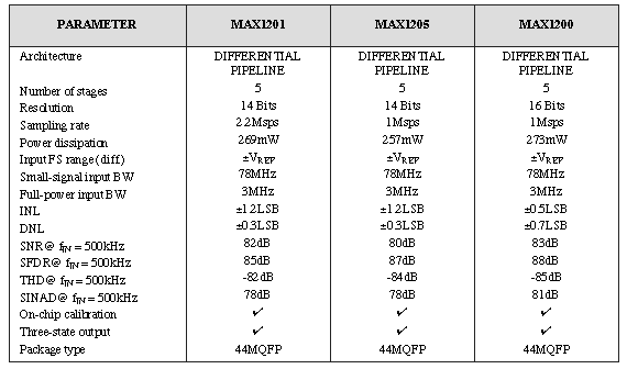
In summary, Table 2 recaps the major ADC types available today. To order Maxim product samples for your evaluation, use the Business Reply Card in this issue.
Table 2. Major analog-to-digital conversion techniques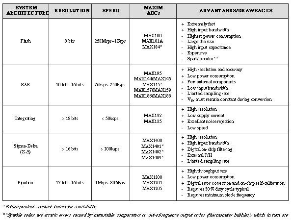
- 相关推荐
- adc
-
ACQT和ADCS值怎么选择2018-12-14 0
-
ADCS=5禁用DONE位?2020-04-08 0
-
跪求Hybrid ADCs Smart Sensors2021-06-22 0
-
ADCS7476/ADCS7477/ADCS7478,pdf2009-10-12 734
-
Pipeline ADCs Come of Age2009-04-25 990
-
流水线模数转换器的时代-Pipeline ADCs Come2009-05-01 982
-
Understanding SAR ADCs2009-05-08 794
-
age文件加密工具2022-05-06 507
-
RJP4010AGE 数据表2023-04-04 104
-
RJP4006AGE 数据表2023-04-20 105
-
SpinalHDL里pipeline的设计思路2023-08-16 713
-
Pipeline中throwIt的用法2023-10-21 280
-
什么是pipeline?Go中构建流数据pipeline的技术2024-03-11 160
全部0条评论

快来发表一下你的评论吧 !
