

Compact DWDM laser Temperature
应用电子电路
807人已加入
描述
Abstract: A complete and very compact thermal control solution for DWDM (Dense Wavelength Division Multiplexing) laser modules can be made using a MAX8520/21 and a single op amp. Because DWDM uses multiple lasers on a single fiber, careful control of the laser output frequencies is required. This design can easily provide the level of performance needed for 25GHz channel spacing making it an ideal foundation for designers working on DWDM fiber optic systems.
A complete and very compact thermal control solution for DWDM (Dense Wavelength Division Multiplexing) laser modules can be made using a MAX8520/21 and a single op amp. Because DWDM uses multiple lasers on a single fiber, careful control of the laser output frequencies is required. A 1548nm DWDM system with 25GHz-channel spacing requires the laser frequency to be held at the center of the 25GHz band. The laser modules must be tuned to mid-band by changing their operating temperature and then held over all time and environmental variations. Because the laser driver can typically change 0.1nm/°C (25GHz/°C) a temperature controller with a stability of at least ±0.1°C is required. This keeps the modulated laser spectrum in the center (±2.5GHz) of the band and limits channel cross talk to a minimum. Venders are promising as many as 160 channels on a single fiber.
Because the laser modules must be set to their mid-band by changing their operating temperature from 15°C to 35°C, and the ambient can vary from 0°C to 70°C, the controller must be capable of heating and cooling. Peltier Thermal-Electric Coolers (TECs) can perform this function but the power driver for the cooler must be capable of bi-directional (both heating and cooling) operation. Furthermore, the driver must not exhibit dead-band or hunting during the transition from heating to cooling modes. The MAX8520/21 is a bi-directional power driver capable of sourcing and sinking up to 1.5 Amps. Using the MAX8520/21 with a temperature monitor (10kΩ thermistor) inside the laser module and a single op amp, a Proportional Integral differential (PID) controller can be implemented as a thermal regulation loop. The circuit block is shown below in Figure 1. A full schematic and parts list can be found at the end of this application note.
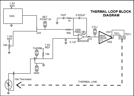
Figure 1. Block diagram for thermal control loop.
In this circuit, JU4 can be configured with a DAC (Digital to Analog Converter) or a potentiometer to set the reference temperature voltage. The op amp then compares the temperature reference voltage against the thermistor voltage and the difference is amplified and fed into the MAX8520/21. The MAX8520/21 outputs a current to reduce the error sensed by the op amp, completing the loop. Because the MAX8520/21 requires a ±1.5 volt signal at CTLI to produce ±1.5 Amps, the op amp must generate this signal from a temperature error at the input. Setting the temperature limit to ±0.1°C, and knowing that the thermistor sensitivity is 14mV/1°C, we can calculate the required op amp gain.
With
0.1°C * 14mV/1°C = 1.4mV
and because
1.4mV * Gain = 1.5V
the op amp gain must be at least 1.1K.
By selecting 50kΩ for the input resistance at the inverting pin of the op amp, it follows that the 10uF integrating capacitor must have impedance of at least 50MΩ. Careful selection of components and layout must be applied to guarantee this gain. Taiyo Yuden specifies 1GΩ/µF for capacitors larger than 1µF. For a 10µF this equates to 100MΩ. The typical measured values are much higher but without proper layout and assembly techniques, moisture or solder flux can easily nullify efforts to achieve high impedance circuit performance. Testing in an environmental chamber at 0°C can cause water to condense and reduce circuit performance. Leakage currents on the PCB (Printed Circuit Board) can also create problems at this impedance level. It is therefore recommended that a guard ring be placed around the inverting input on the op amp and it's associated components. The location of this guard ring is shown this in Figure 2.
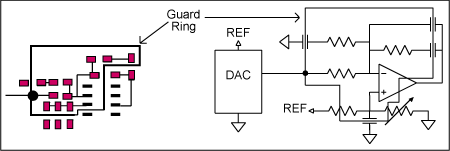
Figure 2. PCB layout for guard ring.
The guard ring functions as follows. Because the DAC output voltage is similar to the op amp's inverting input voltage there is essentially no potential difference between the guard ring and summing junction and its associated components inside the ring. The ring intercepts outside surface leakage currents where they are shunted by the low impedance of the DAC. The low impedance ring protects (or "guards") the high gain summing node from leakage currents. The wider the guard ring trace, the greater effect it will have. A ground plane at the DAC output potential should also be placed on the layer immediately below the sensitive circuit components. Even with the guard ring, water and other surface contaminates can still degrade circuit performance. As a final measure an acrylic based conformal coating should be applied to the cleaned and dried PCB and its components after assembly. PCB assemblers can apply this to the assembled boards if it is specified.
After the op amp generates the error signal, the MAX8520/21 converts the error voltage at the CTLI input to a bipolar output current. The voltage controlled output current of the MAX8520/21 helps to control harmful current surges and provide a programmable current limit. The output current and voltage limits can be independently programmed with external resistors. The MAX8520/21 comes with four power MOSFETs integrated in a small 20 pin QFN package and the ultra small UCSP™ package. Waste heat is expelled through an exposed metal pad on the bottom of the chip, which is then soldered to a copper ground plane on the PCB. The high switching frequency of the MAX8520/21 also helps reduces external component size.
Because of the long thermal time constants exhibit by TEC modules, the control loop must also be slow to maintain stability. The components for the PID loop are selected to provide a 1Hz unity gain crossover. While the DC gain of this loop sets the steady state performance, the AC gain bandwidth of the loop defines the transient response. Achieving the highest stable gain bandwidth will produce the fastest transient response and we know that, with time, the integrator will exponentially reduce the loop error.
While it is true that with infinite gain the steady state error for the PID loop is zero, in transient cases, such as a system warm up, the loop gain is far less than infinite. This is shown in the thermal plots in Figure 3 below. Figure 3 shows the TEC system's response to a temperature step change. For this test the module's internal laser temperature is set to 25°C (Vtherm = 0.75V). The external temperature is changed from 25°C to 45°C in 20 minutes (1°C/Minute) then held for 40 minutes. Finally it is ramped back to 25°C at 1°C/Minute. From Figure 3 we can determine that the thermal error for this transient change is 200µV Pk to Pk, or 15m°C, or ±7.5m°C. At the end of the hold period, the steady state error is less than 50µV Pk to Pk, far less than the transient error. It is important to note that the thermal data in this report shows that the control system can regulate the thermistor's temperature accurately, this may not exactly represent the laser temperature or the light wavelength produced.
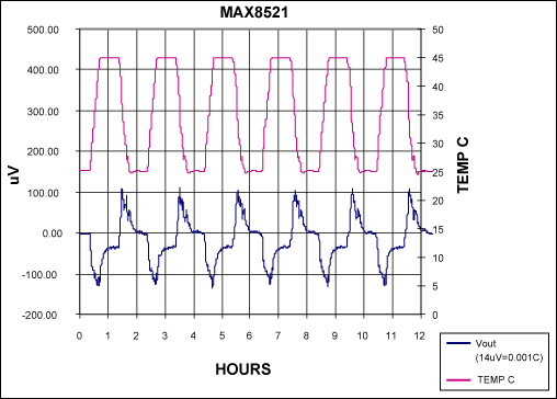
Figure 3. Twelve hour strip chart showing thermal performance of control loop.
Figure 4 shows the system's response to three different external temperature ramps (1, 0.7 and 0.3 degrees per minute). In this test the module's internal temperature is set to 35°C (Vtherm = 0.592V). It is important to note that accurate temperature measurements must be given a long time to settle. In fact with enough time to settle, the plot would follow in the center of the three rates of Figure 4. Figure 5 is the same test as Figure 4 with the internal laser temperature set to 15°C (Vtherm = 0.916V).
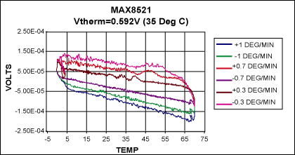
Figure 4. Thermal loop performance for three different rates of temperature change and the module set at 35°C.
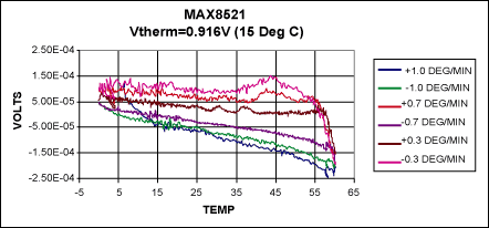
Figure 5. Thermal loop performance for three different rates of temperature change and the module set at 15°C.
When performing thermal tests, it is important to note that water can play a significant role in degrading circuit performance. At 0°C and below water freezes and has no effect on the circuit. When the temperature rises however, the ice melts and the water can cause leakage currents that can reduce the thermal performance. As mentioned above, an acrylic based conformal coating over the circuit can help improve this situation.
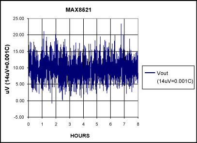
Figure 6. Long term Stability Plot (Maximum error 0.0018°C).
Figure 6 shows a long-term (8 hour) stability plot. This plot shows that the maximum thermal error is 25µV or 1.8m°C. This test is done with a voltmeter taking readings every 10 seconds so the test bandwidth is somewhat limited. A key reason for the excellent stability shown in this test is the MAX4238 Chopper Stabilized Op Amp. Chopper Stabilization holds offset and drift to a minimum. Furthermore, the op amp's shutdown pin is configured in parallel with the MAX8521's enable pin. This is done to limit the startup surge associated with the PID's integrating capacitor starting at the rail potential. Because the MAX4238 has a high output impedance in shut down mode, the CTLI pin of the MAX8521 charges the op amp output and integrating capacitor (C16) to 1.5 Volts, or zero current through the TEC module. The helps very much to limit the start up surge that would otherwise force the TEC module to take full current until the integrating capacitor discharges (20Sec).
Clearly the DWDM fiber optic system will replace single wavelength systems. Most vendors are starting with 100GHz spacing and have plans for 25GHz-channel spacing. Maxim Integrated Product's MAX8520/21 can easily provide the level of performance needed for 25GHz channel spacing making it an ideal foundation for designers working on DWDM fiber optic systems. Maxim is also able to provide the MAX8521 in an ultra small UCSP package, which is small enough to be integrated inside the laser module offering further space savings.
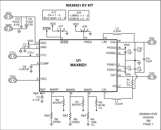
Figure 7.
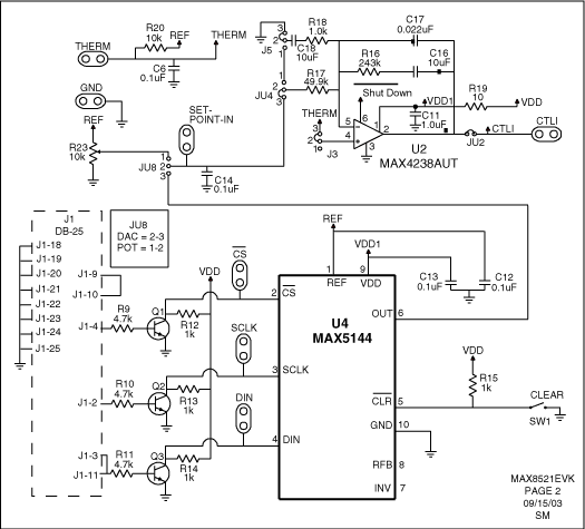
Figure 8.
MAX8521 SINGLE OP AMP DESIGN
打开APP阅读更多精彩内容
A complete and very compact thermal control solution for DWDM (Dense Wavelength Division Multiplexing) laser modules can be made using a MAX8520/21 and a single op amp. Because DWDM uses multiple lasers on a single fiber, careful control of the laser output frequencies is required. A 1548nm DWDM system with 25GHz-channel spacing requires the laser frequency to be held at the center of the 25GHz band. The laser modules must be tuned to mid-band by changing their operating temperature and then held over all time and environmental variations. Because the laser driver can typically change 0.1nm/°C (25GHz/°C) a temperature controller with a stability of at least ±0.1°C is required. This keeps the modulated laser spectrum in the center (±2.5GHz) of the band and limits channel cross talk to a minimum. Venders are promising as many as 160 channels on a single fiber.
Because the laser modules must be set to their mid-band by changing their operating temperature from 15°C to 35°C, and the ambient can vary from 0°C to 70°C, the controller must be capable of heating and cooling. Peltier Thermal-Electric Coolers (TECs) can perform this function but the power driver for the cooler must be capable of bi-directional (both heating and cooling) operation. Furthermore, the driver must not exhibit dead-band or hunting during the transition from heating to cooling modes. The MAX8520/21 is a bi-directional power driver capable of sourcing and sinking up to 1.5 Amps. Using the MAX8520/21 with a temperature monitor (10kΩ thermistor) inside the laser module and a single op amp, a Proportional Integral differential (PID) controller can be implemented as a thermal regulation loop. The circuit block is shown below in Figure 1. A full schematic and parts list can be found at the end of this application note.
Figure 1. Block diagram for thermal control loop.
In this circuit, JU4 can be configured with a DAC (Digital to Analog Converter) or a potentiometer to set the reference temperature voltage. The op amp then compares the temperature reference voltage against the thermistor voltage and the difference is amplified and fed into the MAX8520/21. The MAX8520/21 outputs a current to reduce the error sensed by the op amp, completing the loop. Because the MAX8520/21 requires a ±1.5 volt signal at CTLI to produce ±1.5 Amps, the op amp must generate this signal from a temperature error at the input. Setting the temperature limit to ±0.1°C, and knowing that the thermistor sensitivity is 14mV/1°C, we can calculate the required op amp gain.
With
0.1°C * 14mV/1°C = 1.4mV
and because
1.4mV * Gain = 1.5V
the op amp gain must be at least 1.1K.
By selecting 50kΩ for the input resistance at the inverting pin of the op amp, it follows that the 10uF integrating capacitor must have impedance of at least 50MΩ. Careful selection of components and layout must be applied to guarantee this gain. Taiyo Yuden specifies 1GΩ/µF for capacitors larger than 1µF. For a 10µF this equates to 100MΩ. The typical measured values are much higher but without proper layout and assembly techniques, moisture or solder flux can easily nullify efforts to achieve high impedance circuit performance. Testing in an environmental chamber at 0°C can cause water to condense and reduce circuit performance. Leakage currents on the PCB (Printed Circuit Board) can also create problems at this impedance level. It is therefore recommended that a guard ring be placed around the inverting input on the op amp and it's associated components. The location of this guard ring is shown this in Figure 2.
Figure 2. PCB layout for guard ring.
The guard ring functions as follows. Because the DAC output voltage is similar to the op amp's inverting input voltage there is essentially no potential difference between the guard ring and summing junction and its associated components inside the ring. The ring intercepts outside surface leakage currents where they are shunted by the low impedance of the DAC. The low impedance ring protects (or "guards") the high gain summing node from leakage currents. The wider the guard ring trace, the greater effect it will have. A ground plane at the DAC output potential should also be placed on the layer immediately below the sensitive circuit components. Even with the guard ring, water and other surface contaminates can still degrade circuit performance. As a final measure an acrylic based conformal coating should be applied to the cleaned and dried PCB and its components after assembly. PCB assemblers can apply this to the assembled boards if it is specified.
After the op amp generates the error signal, the MAX8520/21 converts the error voltage at the CTLI input to a bipolar output current. The voltage controlled output current of the MAX8520/21 helps to control harmful current surges and provide a programmable current limit. The output current and voltage limits can be independently programmed with external resistors. The MAX8520/21 comes with four power MOSFETs integrated in a small 20 pin QFN package and the ultra small UCSP™ package. Waste heat is expelled through an exposed metal pad on the bottom of the chip, which is then soldered to a copper ground plane on the PCB. The high switching frequency of the MAX8520/21 also helps reduces external component size.
Because of the long thermal time constants exhibit by TEC modules, the control loop must also be slow to maintain stability. The components for the PID loop are selected to provide a 1Hz unity gain crossover. While the DC gain of this loop sets the steady state performance, the AC gain bandwidth of the loop defines the transient response. Achieving the highest stable gain bandwidth will produce the fastest transient response and we know that, with time, the integrator will exponentially reduce the loop error.
While it is true that with infinite gain the steady state error for the PID loop is zero, in transient cases, such as a system warm up, the loop gain is far less than infinite. This is shown in the thermal plots in Figure 3 below. Figure 3 shows the TEC system's response to a temperature step change. For this test the module's internal laser temperature is set to 25°C (Vtherm = 0.75V). The external temperature is changed from 25°C to 45°C in 20 minutes (1°C/Minute) then held for 40 minutes. Finally it is ramped back to 25°C at 1°C/Minute. From Figure 3 we can determine that the thermal error for this transient change is 200µV Pk to Pk, or 15m°C, or ±7.5m°C. At the end of the hold period, the steady state error is less than 50µV Pk to Pk, far less than the transient error. It is important to note that the thermal data in this report shows that the control system can regulate the thermistor's temperature accurately, this may not exactly represent the laser temperature or the light wavelength produced.
Figure 3. Twelve hour strip chart showing thermal performance of control loop.
Figure 4 shows the system's response to three different external temperature ramps (1, 0.7 and 0.3 degrees per minute). In this test the module's internal temperature is set to 35°C (Vtherm = 0.592V). It is important to note that accurate temperature measurements must be given a long time to settle. In fact with enough time to settle, the plot would follow in the center of the three rates of Figure 4. Figure 5 is the same test as Figure 4 with the internal laser temperature set to 15°C (Vtherm = 0.916V).
Figure 4. Thermal loop performance for three different rates of temperature change and the module set at 35°C.
Figure 5. Thermal loop performance for three different rates of temperature change and the module set at 15°C.
When performing thermal tests, it is important to note that water can play a significant role in degrading circuit performance. At 0°C and below water freezes and has no effect on the circuit. When the temperature rises however, the ice melts and the water can cause leakage currents that can reduce the thermal performance. As mentioned above, an acrylic based conformal coating over the circuit can help improve this situation.
Figure 6. Long term Stability Plot (Maximum error 0.0018°C).
Figure 6 shows a long-term (8 hour) stability plot. This plot shows that the maximum thermal error is 25µV or 1.8m°C. This test is done with a voltmeter taking readings every 10 seconds so the test bandwidth is somewhat limited. A key reason for the excellent stability shown in this test is the MAX4238 Chopper Stabilized Op Amp. Chopper Stabilization holds offset and drift to a minimum. Furthermore, the op amp's shutdown pin is configured in parallel with the MAX8521's enable pin. This is done to limit the startup surge associated with the PID's integrating capacitor starting at the rail potential. Because the MAX4238 has a high output impedance in shut down mode, the CTLI pin of the MAX8521 charges the op amp output and integrating capacitor (C16) to 1.5 Volts, or zero current through the TEC module. The helps very much to limit the start up surge that would otherwise force the TEC module to take full current until the integrating capacitor discharges (20Sec).
Clearly the DWDM fiber optic system will replace single wavelength systems. Most vendors are starting with 100GHz spacing and have plans for 25GHz-channel spacing. Maxim Integrated Product's MAX8520/21 can easily provide the level of performance needed for 25GHz channel spacing making it an ideal foundation for designers working on DWDM fiber optic systems. Maxim is also able to provide the MAX8521 in an ultra small UCSP package, which is small enough to be integrated inside the laser module offering further space savings.
Figure 7.
Figure 8.
MAX8521 SINGLE OP AMP DESIGN
| DESIGNATION | QTY | DESRIPTION |
| C8 | 1 | 0.047µF, 50V, X7R Ceramic Cap. (0402) Murata (GRM36X7R473K10) |
| C17 | 1 | 0.022µF, 50V, X7R, Ceramic Cap.(1206) Kemet (C1206C223K5RACTU) |
| C6, C7, C12-C14 | 5 | 0.1µF 16V X7R Ceramic Cap. (0402) Murata (GRM36X5R104K10) |
| C1-C3, C5, C11, C20 | 6 | 1µF 10V X5R Ceramic Cap. (0603) Taiyo Yuden (JMK107BJ105MG) Murata (GRM188R60J105KA) |
| C4 | 1 | 10µF 6.3V X5R Ceramic Cap. (0805) Taiyo Yuden (JMK212BJ106MG) |
| C9, C16, C18 | 3 | 10µF 6.3V X5R Ceramic Cap. (1206) Taiyo Yuden (JMK316BJ106ML) |
| C21 | 1 | 150µF Electrolytic Cap, Sanyo (10MV150SAX) (Note: 150µF Total Buss Capacitance or Stiff Line Input) |
| L1, L2 | 2 | 2.2µH, 1.6A Inductor Sumida (CDRH2D18-2R2) |
| Q1-Q3 | 3 | NPN Bipolar Transistor, 40V SOT-23 Central Semi. (CMPT3904) |
| R1 | 1 | 0.1Ω, 1%, 0.25W, Sense Resistor (1206) Panasonic ERJ8RSFR10 |
| R19 | 1 | 10Ω 5% resistor (0805) |
| R12-R15, R18 | 5 | 1kΩ 5% resistor (0402) |
| R9-R11 | 3 | 4.7kΩ 5% resistor (0402) |
| R20 | 1 | 10kΩ, 0.1%, 25ppm/C°, resistor (0805), Panasonic, (ERA6YEB103) |
| R3 | 1 | 49.9kΩ 1% resistor (0402) |
| R17 | 1 | 49.9kΩ 5% resistor (1206) |
| R4 | 1 | 100kΩ 1% resistor (0402) |
| R16 | 1 | 240kΩ 5% resistor (0603) |
| R23 | 1 | 10k Potentiometer (multi-turn) Bourn 3266W-1-103 |
| SW1 | 1 | Switch, Momentary, NO Mouser (101-0010) |
| U2 | 1 | Op Amp, (SOT23-6) Maxim (MAX4238AUT) |
| U4 | 1 | Serial 14 Bit DAC (10-pin µMAX®) Maxim (MAX5144EUB) |
| U1 | 1 | Power Driver (20-Pin THIN QFN) Maxim (MAX8521ETP) |
µMAX is a registered trademark of Maxim Integrated Products, Inc.
UCSP is a trademark of Maxim Integrated Products, Inc.
声明:本文内容及配图由入驻作者撰写或者入驻合作网站授权转载。文章观点仅代表作者本人,不代表电子发烧友网立场。文章及其配图仅供工程师学习之用,如有内容侵权或者其他违规问题,请联系本站处理。
举报投诉
- 相关推荐
- DWDM
-
超大容量智能DWDM传输平台jf_02447348 2023-02-07
-
Features of laser diodes2009-05-12 0
-
什么是Compact PCI?2009-06-14 0
-
什么是dwdm光模块?有哪些应用?2018-03-27 0
-
什么是DWDM密集型光波复用?DWDM产品有哪些?2018-03-30 0
-
CWDM/DWDM系统应用方案2020-12-07 0
-
MAX3736,pdf (SFP Laser Driver)2010-09-23 889
-
HFAN-08.2.1: PWM Temperature C2009-04-17 2697
-
密集波分复用激光温度控制与MAX8521-Compact D2009-04-22 2057
-
DWDM(密集波分复用),DWDM是什么意思2010-03-19 8725
-
DWDM技术、原理与应用6-12章2016-04-25 639
-
sc400-4-compact数据手册2016-12-25 584
-
什么是DWDM光模块,它的优势有哪些2021-08-24 1828
-
DWDM光模块是什么?常见DWDM光模块类型 与普通光模块有什么区别?2023-12-27 330
全部0条评论

快来发表一下你的评论吧 !
