

DS2152, DS2154, DS21x5Y, and D
通信设计应用
58人已加入
描述
Abstract: Application note 319 contains information necessary to interface the Motorola MC68360 processor to many of the Dallas Semiconductor single chip transceivers (SCTs). The application note covers interfacing both the address and data processor bus and the communications serial bus. Interfacing the processor bus of the MC68360 to the SCT is straightforward and mapping of address and data lines are shown in detail. Depending on the application, it may be necessary to add external logic to latch the address and data pins isolate other peripheral on the processor bus. The MC68360 contains two serial interfaces, either of which can be used to communicate directly with the SCT. The communication serial bus pin, clock names and descriptions for the MC68360 are located in diagrams in the application note. An example circuit diagram is provided for the processor interface as well as the communication serial interface. The goal of the application note is to give the designer enough information to begin a design based on the MC68360 processor.
However, the DS2152, DS21x52 and DS2155 have a built-in HDLC controller for the T1 FDL. Any combination of the QUICC32's SCCs and SMCs can be processed through an internal timeslot assignor onto one or two time-division multiplex channels, TDMA and TDMB. In the configuration shown, TDM channel A is used for timeslots 0 to 23 (T1) or 0 to 31 (E1), and TDM channel B is used optionally for the Sa bit (E1). Refer to the MC68360 Quad Integrated Communications Controller User's Manual for complete details.
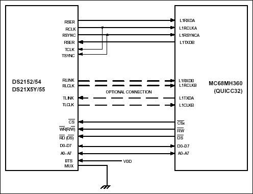
Figure 1. DS2152, DS2154, DS21x5Y, or DS2155–QUICC32 Interconnections.
DS2152, DS2154, DS21x5Y, and DS2155 Notes:
打开APP阅读更多精彩内容
Overview
Interconnections between the DS2152, DS2154, DS21x5Y, or DS2155 and the Motorola MC68MH360 (QUICC32) are shown in Figure 1. The MC68MH360 can be configured as an HDLC controller implementing protocols such as LAPD for T1 FDL, DS0 channel SS7, or the E1 Sa bits.However, the DS2152, DS21x52 and DS2155 have a built-in HDLC controller for the T1 FDL. Any combination of the QUICC32's SCCs and SMCs can be processed through an internal timeslot assignor onto one or two time-division multiplex channels, TDMA and TDMB. In the configuration shown, TDM channel A is used for timeslots 0 to 23 (T1) or 0 to 31 (E1), and TDM channel B is used optionally for the Sa bit (E1). Refer to the MC68360 Quad Integrated Communications Controller User's Manual for complete details.
Figure 1. DS2152, DS2154, DS21x5Y, or DS2155–QUICC32 Interconnections.
DS2152, DS2154, DS21x5Y, and DS2155 Notes:
- Other signals affecting operation of device are not shown.
- Example circuit has RSYNC in output mode.
- Other signals affecting operation of device are not shown.
- Use SI mode register t
- Set up transmit and receive frame-sync delays (0 to 3 clocks) to mask the F-bit in T1 applications.
- Set clock edges for transmit on rising edge and receive on falling edge. CEA = CEB = 0.
- In the above example, TDM channel A has a common transmit/receive clock and sync. CTRA = 1. Use the TIMESLOT ASSIGNER to ignore Timeslot 0 for E1 mode.
声明:本文内容及配图由入驻作者撰写或者入驻合作网站授权转载。文章观点仅代表作者本人,不代表电子发烧友网立场。文章及其配图仅供工程师学习之用,如有内容侵权或者其他违规问题,请联系本站处理。
举报投诉
-
DS2151, DS2152, DS2153, DS21542009-04-20 788
-
DS2152, DS2154, DS2151, DS21532009-04-20 804
-
DS21352/DS21552 versus DS21522009-04-20 678
-
DS2152, DS2154 Clock Map2009-04-20 830
-
Converting the DS2152/DS2154 D2009-04-20 777
-
DS2152, DS2154 Interfacing to2009-04-20 631
-
Tech Brief 7: DS2152 and DS2152009-04-20 1077
-
DS21Q4x, DS215x, and DS21x5y T2009-04-20 935
-
DS2152,DS2154时钟地图-DS2152, DS212009-04-29 1548
-
转换DS2152/DS2154演示套件-Converting2009-04-29 1096
-
DS2152 and DS2154 8MHz System2009-04-29 1043
-
为下一代器件提供DS2152或DS2154硬件设计2023-01-13 604
全部0条评论

快来发表一下你的评论吧 !
