
接口1多路复用总线实时时钟到μP单独地址和数据总线-Inte
通信设计应用
62人已加入
描述
Abstract: This application note provides general information about how to interface a real-time clock (RTC) that has a multiplexed-bus (multiplexed address and data) interface (example: DS12887) with a microcontroller that has separate address and data buses.
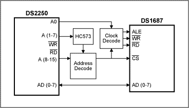
An IC multiplexed-bus real-time clock (RTC) is designed for use with processors that include a multiplexed data-address bus, but some designers prefer to use such "mux-bus" RTCs with processors whose data and address buses are separate (Figure 1).

Figure 1. The components shown interface a mux-bus RTC to a processor (DS2250) with separate data and address buses.
The mux-bus RTC has four control signals. Chip Select (active-low CS) must be active when reading or writing data. Read Data strobe (active-low RD) is for data reads, Write Data strobe (active-low WR) is for data writes, and Address Strobe (ALE) latches the register address internally. The falling edge of ALE latches the register address (presented on pins AD0-AD7 of the Address/Data bus) whenever active-low RD and active-low WR are both high. You then transfer data to or from the selected clock register via AD0-AD7 by toggling active-low WR or active-low RD low while active-low CS is active.
In Figure 1, the interface between the RTC (DS1687) and an 8051-type processor (DS2250) ignores the expanded memory multiplexed address and data function provided by the processor's P0, P2 and ALE pins (not shown). Instead, external logic creates the ALE signal, and the RTC is memory-mapped into the expanded memory area.
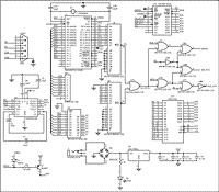
The configuration above requires two address locations in the processor address space. When A0 is low, the clock-decode logic toggles ALE while active-low RD and active-low WR are held high. When A0 is high, the clock-decode logic holds ALE low while toggling active-low RD or active-low WR low. The address-decode logic holds active-low CS low for either state of A0, provided A1-15 matches the address to which the clock is mapped. In software, you access the clock by writing the register address to the lower address (A0 low), which is followed by a read or write to the upper address (A0 high). The associated software can be downloaded from the Maxim site. Figure 2 shows the complete schematic.

For Larger Image
Figure 2.
打开APP阅读更多精彩内容
An IC multiplexed-bus real-time clock (RTC) is designed for use with processors that include a multiplexed data-address bus, but some designers prefer to use such "mux-bus" RTCs with processors whose data and address buses are separate (Figure 1).

Figure 1. The components shown interface a mux-bus RTC to a processor (DS2250) with separate data and address buses.
The mux-bus RTC has four control signals. Chip Select (active-low CS) must be active when reading or writing data. Read Data strobe (active-low RD) is for data reads, Write Data strobe (active-low WR) is for data writes, and Address Strobe (ALE) latches the register address internally. The falling edge of ALE latches the register address (presented on pins AD0-AD7 of the Address/Data bus) whenever active-low RD and active-low WR are both high. You then transfer data to or from the selected clock register via AD0-AD7 by toggling active-low WR or active-low RD low while active-low CS is active.
In Figure 1, the interface between the RTC (DS1687) and an 8051-type processor (DS2250) ignores the expanded memory multiplexed address and data function provided by the processor's P0, P2 and ALE pins (not shown). Instead, external logic creates the ALE signal, and the RTC is memory-mapped into the expanded memory area.
The configuration above requires two address locations in the processor address space. When A0 is low, the clock-decode logic toggles ALE while active-low RD and active-low WR are held high. When A0 is high, the clock-decode logic holds ALE low while toggling active-low RD or active-low WR low. The address-decode logic holds active-low CS low for either state of A0, provided A1-15 matches the address to which the clock is mapped. In software, you access the clock by writing the register address to the lower address (A0 low), which is followed by a read or write to the upper address (A0 high). The associated software can be downloaded from the Maxim site. Figure 2 shows the complete schematic.

For Larger Image
Figure 2.
声明:本文内容及配图由入驻作者撰写或者入驻合作网站授权转载。文章观点仅代表作者本人,不代表电子发烧友网立场。文章及其配图仅供工程师学习之用,如有内容侵权或者其他违规问题,请联系本站处理。
举报投诉
-
EnCoReV中的I/O模拟多路复用器2019-05-07 0
-
具有总线缓冲器的引脚可选,2通道,2线多路复用器2019-05-09 0
-
总线多路复用器LTC4305相关资料分享2021-03-23 0
-
PCF8563P实时时钟芯片参数资料推荐2021-04-28 0
-
利用I2C总线被驱动为低电平但不起作用如何解决2022-12-08 0
-
多路复用技术2009-06-27 969
-
基于CPLD的非多路复用与多路复用总线转换桥的设计与实现2009-03-28 834
-
非多路复用与多路复用总线转换桥的设计与实现2009-03-28 936
-
HYM8563低功耗CMOS实时时钟日历芯片的数据手册免费下载2019-03-28 1791
-
ADG3249:2.5 V/3.3 V,2:1多路复用器/多路分解器总线开关数据表2021-04-29 558
-
ADG3248:2.5 V/3.3 V,2:1多路复用器/多路分解器总线开关数据表2021-04-29 761
-
LTC4305:带电容缓冲的2通道、2线总线多路复用器数据表2021-05-08 527
-
LTC4306:带电容缓冲的4通道2线总线多路复用器数据表2021-05-08 554
-
DS2141A、DS2143、DS2151、DS2153与非多路复用总线接口2023-02-09 853
全部0条评论

快来发表一下你的评论吧 !

