

原型与表面贴装器件-Prototyping with Sur
电子技术
47人已加入
描述
Abstract: Surface mount devices can often be prototyped without etched PCBs by using plain copperclad and simple cutting tools.
As surface-mount technology (SMT) has become more prevalent (and many devices are only available in surface-mount), prototyping techniques have changed.
Many engineers and technicians are comfortable with through-hole devices, perforated fiberglass boards, IC sockets, and wire-wrap or point-to-point wiring. Prototyping with surface-mount devices requires different materials and tools. In some ways, these techniques are easier, once the proper skills have been developed.
This application note presents prototyping methods for surface-mount ICs. This technique is readily used for ICs with a lead pitch down to 0.05 inches (1.27 mm), and with practice can be used down to 0.025 inches (0.64 mm), so it works for well SOICs and virtually all passive SMT components.
The basic idea is to cut narrow slots in a copper-clad board, creating rectangular pads, and place the components across the slots. Each rectangular pad is a node in the circuit. It requires copper-clad board and a rotary hand held grinding tool, plus a few other basic tools.
To illustrate this technique the circuit of Figure 1, a 5 Watt DC-DC step-down voltage converter, is constructed.

Figure 1. This DC-DC converter circuit is used to illustrate SMT prototyping technique.
Start with a fully annotated schematic and gather the parts so you have a good idea of their relative sizes. It is also helpful to have the pin configuration drawings for any ICs in the circuit. Use blank paper, and two pencils of different colors to make a rough drawing of the physical circuit layout. An eraser is essential, and quite often a few iterations are required. Make the drawing larger than life, but stay more-or-less true to scale. You don't need to be very picky with size, but placement matters. Use the lighter color to draw the component outlines, placing parts that share a node close together where practical.
Once all the part outlines are drawn, use the darker color to draw lines separating the different nodes of the circuit (Figure 2). A typical line will go around a few IC pads, "through" a resistor, and back around (the resistor will straddle the line). The lines represent where cuts to the copper-clad will be made. If only straight lines and 90° turns are used, it makes the cutting easier.
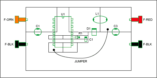
Figure 2. Layout drawing for the SMT prototype of the circuit in Figure 1, showing the component outlines (green) and the node outlines (black). Note that the components bridge the node outlines.
Note that in the circuit implemented here, one jumper wire is used, connecting U1-8 to the output node. The connection could be cut into the copper-clad, but doing so would either interrupt the ground plane or force the trace to run under the IC, neither being desirable. On a multi-layer circuit board the trace would likely be placed on a different layer.
To transfer the layout to the copper-clad board, set the board on a flat surface and place the components on it, using the drawing as a guide. With an awl or other sharp object to bore a small dot into the copper-clad at points corresponding to the end of each dark line segment in the drawing. This takes some practice because all those little parts tend to bounce around. After all the dots are in place, scribe lines into the copper-clad, connecting the dots as indicated by the drawing.
Now cut the slots into the board. Use a roto-tool with a small, flat tip bit (a Dremel® bit #194 works well, see Figure 3), to cut slots into the copper-clad along the scribed lines. This will also take a little practice. After all the slots are finished, go over them with an X-Acto® knife to cut away any pesky little shorts, double checking the corners where burrs are usually the worst. A once-over with some Scotch-Brite® adds a nice finishing touch. Wash and dry the board, and then use an Ohmmeter to verify that no pad is shorted to any of its neighbors. Now all that's left is to install the components and test the circuit. Figure 4 shows a photo of the slotted board, and Figure 5 shows the finished product.
Figure 3. Example of a roto-tool bit useful for cutting slots into copper-clad board. Shown is Dremel bit #194.
Figure 4. The cut circuit board, made using copper-clad and a roto-tool, realizes the layout drawing of Figure 2.
Figure 5. The finished SMT prototype circuit board, a working version of the Figure 1 schematic.
One of the nice features of this technique is the natural ground plane that usually emerges. If you are combining SMT and through-hole technology, through-hole devices can be easily adapted to mount on copper-clad by splaying their legs and soldering them down. Prototyping with SMT is not difficult, and with a little practice many prefer it to wire-wrap or point-to-point wiring.
打开APP阅读更多精彩内容
As surface-mount technology (SMT) has become more prevalent (and many devices are only available in surface-mount), prototyping techniques have changed.
Many engineers and technicians are comfortable with through-hole devices, perforated fiberglass boards, IC sockets, and wire-wrap or point-to-point wiring. Prototyping with surface-mount devices requires different materials and tools. In some ways, these techniques are easier, once the proper skills have been developed.
This application note presents prototyping methods for surface-mount ICs. This technique is readily used for ICs with a lead pitch down to 0.05 inches (1.27 mm), and with practice can be used down to 0.025 inches (0.64 mm), so it works for well SOICs and virtually all passive SMT components.
The basic idea is to cut narrow slots in a copper-clad board, creating rectangular pads, and place the components across the slots. Each rectangular pad is a node in the circuit. It requires copper-clad board and a rotary hand held grinding tool, plus a few other basic tools.
To illustrate this technique the circuit of Figure 1, a 5 Watt DC-DC step-down voltage converter, is constructed.
Figure 1. This DC-DC converter circuit is used to illustrate SMT prototyping technique.
Start with a fully annotated schematic and gather the parts so you have a good idea of their relative sizes. It is also helpful to have the pin configuration drawings for any ICs in the circuit. Use blank paper, and two pencils of different colors to make a rough drawing of the physical circuit layout. An eraser is essential, and quite often a few iterations are required. Make the drawing larger than life, but stay more-or-less true to scale. You don't need to be very picky with size, but placement matters. Use the lighter color to draw the component outlines, placing parts that share a node close together where practical.
Once all the part outlines are drawn, use the darker color to draw lines separating the different nodes of the circuit (Figure 2). A typical line will go around a few IC pads, "through" a resistor, and back around (the resistor will straddle the line). The lines represent where cuts to the copper-clad will be made. If only straight lines and 90° turns are used, it makes the cutting easier.
Figure 2. Layout drawing for the SMT prototype of the circuit in Figure 1, showing the component outlines (green) and the node outlines (black). Note that the components bridge the node outlines.
Note that in the circuit implemented here, one jumper wire is used, connecting U1-8 to the output node. The connection could be cut into the copper-clad, but doing so would either interrupt the ground plane or force the trace to run under the IC, neither being desirable. On a multi-layer circuit board the trace would likely be placed on a different layer.
To transfer the layout to the copper-clad board, set the board on a flat surface and place the components on it, using the drawing as a guide. With an awl or other sharp object to bore a small dot into the copper-clad at points corresponding to the end of each dark line segment in the drawing. This takes some practice because all those little parts tend to bounce around. After all the dots are in place, scribe lines into the copper-clad, connecting the dots as indicated by the drawing.
Now cut the slots into the board. Use a roto-tool with a small, flat tip bit (a Dremel® bit #194 works well, see Figure 3), to cut slots into the copper-clad along the scribed lines. This will also take a little practice. After all the slots are finished, go over them with an X-Acto® knife to cut away any pesky little shorts, double checking the corners where burrs are usually the worst. A once-over with some Scotch-Brite® adds a nice finishing touch. Wash and dry the board, and then use an Ohmmeter to verify that no pad is shorted to any of its neighbors. Now all that's left is to install the components and test the circuit. Figure 4 shows a photo of the slotted board, and Figure 5 shows the finished product.
Figure 3. Example of a roto-tool bit useful for cutting slots into copper-clad board. Shown is Dremel bit #194.
Figure 4. The cut circuit board, made using copper-clad and a roto-tool, realizes the layout drawing of Figure 2.
Figure 5. The finished SMT prototype circuit board, a working version of the Figure 1 schematic.
One of the nice features of this technique is the natural ground plane that usually emerges. If you are combining SMT and through-hole technology, through-hole devices can be easily adapted to mount on copper-clad by splaying their legs and soldering them down. Prototyping with SMT is not difficult, and with a little practice many prefer it to wire-wrap or point-to-point wiring.
Scotch-Brite is a registered trademark of 3M.
X-Acto is a registered trademark of Elmer's Products, Inc.
声明:本文内容及配图由入驻作者撰写或者入驻合作网站授权转载。文章观点仅代表作者本人,不代表电子发烧友网立场。文章及其配图仅供工程师学习之用,如有内容侵权或者其他违规问题,请联系本站处理。
举报投诉
-
分析表面贴装PCB板的设计要求2012-10-23 0
-
表面贴装的GDT2013-10-12 0
-
表面贴装印制板的设计技巧2013-10-15 0
-
SMT工艺---表面贴装及工艺流程2016-05-24 0
-
电子表面贴装技术SMT解析2018-09-14 0
-
元器件的贴装性能2018-11-22 0
-
表面贴装检测器材与方法2018-11-22 0
-
三类表面贴装方法2018-11-26 0
-
smt表面贴装技术2018-11-26 0
-
简单的表面贴装闪存Vpp发生器2019-07-04 0
-
普通表面贴装的焊盘和通孔封装的FET/IGBT功率晶体管2020-06-17 0
-
表面贴装印制板的设计技巧有哪些?2021-04-25 0
-
表面贴装元件相关资料下载2021-05-28 0
全部0条评论

快来发表一下你的评论吧 !
