

Switching Between Battery and
开关电源
351人已加入
描述
Abstract: The following application note discusses a circuit that switches power sources efficiently without switching noise using the MAX6326. It discusses the advantages of using this technique over a simple diode-ord method.
Portable equipment that can operate from a battery pack or an external power source (such as a wall-adapter or external supply) needs to be able to smoothly switch between the two power sources. This application note describes a circuit (Figure 1) that switches power sources with good efficiency and without switching noise.
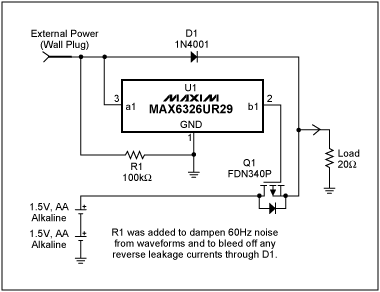
Figure 1. This circuit provides battery/wall-source switchover while debouncing the wall-source output.
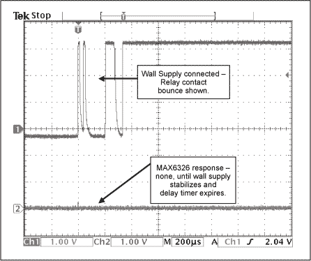
Figure 2. In Figure 1, the U1 output (bottom trace) remains unaffected as the wall-source voltage (top trace) is asserted.
The FET shown in Figure 1 was selected for its low Rds(on) and low Vgs, which is specified down to 1.8V. Thus, the FET can respond to a nearly discharged battery pack of two AA cells (0.9V each).
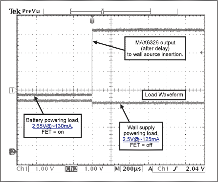
Figure 3. A 20Ω load in Figure 1 (bottom trace) registers a slight mismatch as the wall supply takes over from the battery, indicated (top trace) by the change in U1 output.
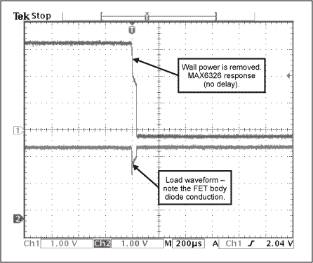
Figure 4. As wall power is removed in Figure 1 (indicated by U1's response in the top trace), the load response (bottom trace) shows the effect of a voltage drop across Q1's body diode.
U1's push-pull active-low output drives the gate of Q1 directly, without external components. If U1's time-out delay is too long, consider the pin-compatible MAX6801 (SOT23 package) or MAX6381 (SC70 package), which offer delay options of 1mS, 20mS, and higher. Another pin-compatible option is the MAX6375 voltage detector (SC-70 package). It provides no time-out delay, but incurs minimal back-drive effects on the battery.
Note that Q1 is reverse-connected with its drain to the battery and its source to the load, which allows its internal body diode to provide the initial current path to the load. At the same time, it blocks the wall supply from uncontrolled charging (back-driving) of the AA cells when Q1 is turned off.
A similar version of this article appeared in the May 13, 2002 issue of Electronic Design magazine.
打开APP阅读更多精彩内容
Portable equipment that can operate from a battery pack or an external power source (such as a wall-adapter or external supply) needs to be able to smoothly switch between the two power sources. This application note describes a circuit (Figure 1) that switches power sources with good efficiency and without switching noise.
Figure 1. This circuit provides battery/wall-source switchover while debouncing the wall-source output.
Power Switching Problems
Two problems are addressed. First, contact bounce effects can occur when the external source is connected and disconnected, resulting in power spikes, as shown in Figure 2. Second, the switching method can introduce a voltage drop, reducing efficiency and battery life.Figure 2. In Figure 1, the U1 output (bottom trace) remains unaffected as the wall-source voltage (top trace) is asserted.
Reducing Voltage Drop
A diode-OR connection is a common solution but the forward voltage drop of the diode limits efficiency. For a small battery pack of one to three cells, the voltage drop for a standard diode (0.6V to 0.7V) is a large percentage of the battery's terminal voltage. The use of a Schottky diode (0.3V to 0.5V drop) improves matters somewhat, but a FET switch can reduce the drop to less than 0.1V.The FET shown in Figure 1 was selected for its low Rds(on) and low Vgs, which is specified down to 1.8V. Thus, the FET can respond to a nearly discharged battery pack of two AA cells (0.9V each).
Reducing Switching Noise
The microprocessor-supervisory circuit (U1 in Figure 1) acts as a wall-source detector and debouncer. It monitors the wall supply and switches from battery power to the wall supply only when the wall supply is stable and has been at or above U1's trip voltage for a period of time. The battery will be back-driven (charged) during this delay period, which is typically 185mS. In Figure 1, note the effect on load voltage when switching from the battery to the wall supply (Figure 3) and vice versa (Figure 4).Figure 3. A 20Ω load in Figure 1 (bottom trace) registers a slight mismatch as the wall supply takes over from the battery, indicated (top trace) by the change in U1 output.
Figure 4. As wall power is removed in Figure 1 (indicated by U1's response in the top trace), the load response (bottom trace) shows the effect of a voltage drop across Q1's body diode.
U1's push-pull active-low output drives the gate of Q1 directly, without external components. If U1's time-out delay is too long, consider the pin-compatible MAX6801 (SOT23 package) or MAX6381 (SC70 package), which offer delay options of 1mS, 20mS, and higher. Another pin-compatible option is the MAX6375 voltage detector (SC-70 package). It provides no time-out delay, but incurs minimal back-drive effects on the battery.
Note that Q1 is reverse-connected with its drain to the battery and its source to the load, which allows its internal body diode to provide the initial current path to the load. At the same time, it blocks the wall supply from uncontrolled charging (back-driving) of the AA cells when Q1 is turned off.
A similar version of this article appeared in the May 13, 2002 issue of Electronic Design magazine.
声明:本文内容及配图由入驻作者撰写或者入驻合作网站授权转载。文章观点仅代表作者本人,不代表电子发烧友网立场。文章及其配图仅供工程师学习之用,如有内容侵权或者其他违规问题,请联系本站处理。
举报投诉
-
switching power supply (SMPS)开关频率2009-04-08 0
-
LI FE Battery study!!!!2015-06-29 0
-
Battery spec!!!!!!!!!!2015-06-29 0
-
我用了between2016-05-15 0
-
Battery charger and method of2009-11-28 502
-
DC DC Power Switching Regulato2009-12-07 766
-
Switching Frame Mode In Live T2009-04-20 1055
-
Switching VGA Signals in a Not2009-04-20 703
-
A Comparison between Battery B2009-04-24 708
-
Step-Up Supply Charges Battery2009-04-30 1340
-
One-Hour Battery Charger Has S2009-04-30 1191
-
Switching Between Battery and2009-05-04 1595
-
Ni-MH Battery2009-11-21 2755
-
Battery/charger load switch approximates ideal diode2011-02-13 4489
全部0条评论

快来发表一下你的评论吧 !
