

RS-485的数据介面可以让孤立的,全双工运作-RS-485
通信设计应用
58人已加入
描述
Abstract: A circuit is described that provides fully isolated RS-485 full-duplex data communication with only two integrated circuits (ICs). An internal transformer-coupled isolated supply and internal optocouplers in the data path provide typical isolation to 1600Vrms for 1 minute or 2000Vram for 1 second. Data rates of 250kbaud are achieved with internally slew-rate-limited circuits or to 2.5Mbaud with non-slew-rate limited circuits, depending upon choice of available ICs.
The simple RS-485 circuit of Figure 1 provides full-duplex communications (simultaneous transmission and reception) with only two essential packages (IC2 and IC3). Its balanced and differential data lines are necessary for high-noise environments or for long-distance transmission between a computer and its peripherals. Such transmissions are difficult, if not impossible, with the single-ended circuitry of an RS-232 transceiver.
The RS-485 standard allows for bidirectional, multi-point, party-line communications, with data rates to 10M bits/second (10Mbps) and line lengths to 1200 meters. Differential transmission provides noise immunity. The circuit shown features controlled-slew-rate drivers that minimize EMI and the reflections caused by improperly terminated cables. It also enables error-free transmissions to 250kbps. To achieve data rates to 2.5Mbps, substitute a full-slew-rate MAX1480A for IC2, a MAX485 for IC3, and R2—R5 values per Table 1.
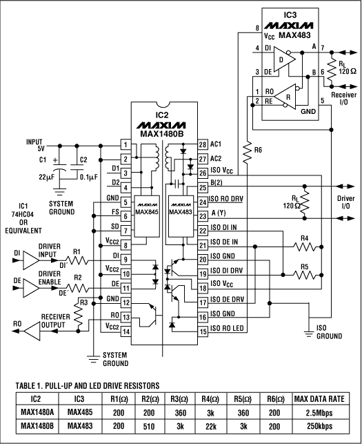
Figure 1. IC2 and IC3 provide full-duplex data communications for cable lengths as long as 1200 meters.
IC2 is a complete half-duplex interface that includes transceivers, optocouplers, a power driver, and a transformer. The optocouplers transmit digital signals across the internal isolation barrier, and the center-tapped transformer transmits power across the barrier from its logic (non-isolated) side to its isolated side.
IC3, powered by the isolated VCC, upgrades the half-duplex operation of IC2 to full duplex using IC2's own dedicated optocouplers. Pin 3 must be tied low to disable IC3's driver, and pin 4 should be left floating. The driver outputs for IC2 and IC3 exhibit high impedance when active-low DE is low; bringing active-low DE high enables the outputs to function as line drivers.
The isolation barrier in IC2 typically withstands 1600Vrms for one minute or 2000Vrms for one second. Any TTL/CMOS-logic family can drive the IC2 digital inputs through a series resistor. With resistive pull-ups, the receiver outputs can drive any such logic as well. IC2's isolated outputs meet all RS-485 specifications.
打开APP阅读更多精彩内容
The simple RS-485 circuit of Figure 1 provides full-duplex communications (simultaneous transmission and reception) with only two essential packages (IC2 and IC3). Its balanced and differential data lines are necessary for high-noise environments or for long-distance transmission between a computer and its peripherals. Such transmissions are difficult, if not impossible, with the single-ended circuitry of an RS-232 transceiver.
The RS-485 standard allows for bidirectional, multi-point, party-line communications, with data rates to 10M bits/second (10Mbps) and line lengths to 1200 meters. Differential transmission provides noise immunity. The circuit shown features controlled-slew-rate drivers that minimize EMI and the reflections caused by improperly terminated cables. It also enables error-free transmissions to 250kbps. To achieve data rates to 2.5Mbps, substitute a full-slew-rate MAX1480A for IC2, a MAX485 for IC3, and R2—R5 values per Table 1.
Figure 1. IC2 and IC3 provide full-duplex data communications for cable lengths as long as 1200 meters.
IC2 is a complete half-duplex interface that includes transceivers, optocouplers, a power driver, and a transformer. The optocouplers transmit digital signals across the internal isolation barrier, and the center-tapped transformer transmits power across the barrier from its logic (non-isolated) side to its isolated side.
IC3, powered by the isolated VCC, upgrades the half-duplex operation of IC2 to full duplex using IC2's own dedicated optocouplers. Pin 3 must be tied low to disable IC3's driver, and pin 4 should be left floating. The driver outputs for IC2 and IC3 exhibit high impedance when active-low DE is low; bringing active-low DE high enables the outputs to function as line drivers.
The isolation barrier in IC2 typically withstands 1600Vrms for one minute or 2000Vrms for one second. Any TTL/CMOS-logic family can drive the IC2 digital inputs through a series resistor. With resistive pull-ups, the receiver outputs can drive any such logic as well. IC2's isolated outputs meet all RS-485 specifications.
声明:本文内容及配图由入驻作者撰写或者入驻合作网站授权转载。文章观点仅代表作者本人,不代表电子发烧友网立场。文章及其配图仅供工程师学习之用,如有内容侵权或者其他违规问题,请联系本站处理。
举报投诉
- 相关推荐
- RS-485
-
采用ADM2582E/ADM2587E实现完全半/全双工的RS-485/RS-422接口隔离2010-04-01 0
-
通讯接口的小知识 ---RS-232、RS-422、RS-485区别2014-06-22 0
-
半双工非隔离式 RS-485 BoosterPack 参考设计2015-05-05 0
-
RS-232、RS-422和RS-485串行数据接口标准2019-04-23 0
-
什么是RS-485多机通信方案?2019-09-29 0
-
使用RS-422和RS-485进行便捷,可靠的数据传输2020-09-18 0
-
RS-485通讯协议的介绍2021-08-20 0
-
RS-485通信相关资料分享2021-09-09 0
-
使用RS-485需要注意什么2021-12-08 0
-
RS-485的相关资料分享2022-02-09 0
-
具有±80V故障保护的全双工RS-485收发器,省去了外部保2008-08-18 884
-
总线之RS-485的工业应用2017-11-16 2039
-
AN-1493:半双工隔离RS-485接口2021-04-23 589
-
UG-543:全双工和半双工RS-485收发器评估板2021-05-24 619
-
【RS-485收发切换】使用RS-485要注意的一个问题2021-11-25 883
全部0条评论

快来发表一下你的评论吧 !
