

Mathcad Calculates Input Capac
电源新闻
19人已加入
描述
Abstract: Step-down buck regulators are extremely popular in a variety of portable and non-portable equipment. These buck converters are terminated with an input capacitor, CIN and an output capacitor, CO, at the output. CIN provides high-frequency filtering, so that VIN has low ripple. This application note helps a system designer to set-up Mathcad and compute CIN for a particular step-down DC-DC regulator design.
Step-down buck regulators are used in portable and non-portable equipment, such as PDAs, cell phones, computers, telcom/networks, and consumer products. These buck converters are terminated with an input capacitor, CIN, at the input, and an output capacitor, CO, at the output. The function of both capacitors is to provide high-frequency filtering, so that VIN and VO are close to pure DC, with little ripple noise.
A capacitor is often represented by a series combination of R, L, and C. R is the equivalent series resistance (ESR) and L is the equivalent series inductance (ESL). The term C is equal to the ideal capacitor value.
Figure 1 shows a typical schematic of a synchronous buck power stage and the associated waveforms to be used for the derivations and calculations.
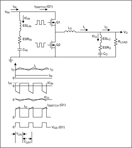
Figure 1. Typical synchronous buck power and waveforms.
As seen in Figure 1, the output ripple current through the input capacitor results in voltage across CIN that reflects the values of ESR, ESL, and C. The ESR and ESL cause fast step voltage rise and fall, whereas C has a linear voltage rise and fall due to the fact that the capacitor charges and discharges. At the start of TON, CIN sees a negative step current, which will produce a negative step voltage given by the following equation:
Another parameter that needs to be determined is the RMS current through the input capacitor, so that the capacitor IRMS rating is not exceeded. From the ICIN waveform, the RMS current can be approximated (since the peak-to-peak inductor ripple current is usually 20-30% of IO max) to be: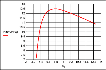
Figure 2.
Due to the high di/dt and pulsating current, a ceramic capacitor is chosen, for its low ESR and ESL. A higher ripple current rating is required at high-frequency to contain the switching spikes. Make sure the RMS current rating of the capacitor is well above the maximum operating RMS current. For long-term reliability, choose a capacitor that will exhibit less than a 10°C temperature rise. Most capacitor manufacturers provide plots that show RMS current vs. temperature rise.
打开APP阅读更多精彩内容
Step-down buck regulators are used in portable and non-portable equipment, such as PDAs, cell phones, computers, telcom/networks, and consumer products. These buck converters are terminated with an input capacitor, CIN, at the input, and an output capacitor, CO, at the output. The function of both capacitors is to provide high-frequency filtering, so that VIN and VO are close to pure DC, with little ripple noise.
A capacitor is often represented by a series combination of R, L, and C. R is the equivalent series resistance (ESR) and L is the equivalent series inductance (ESL). The term C is equal to the ideal capacitor value.
Figure 1 shows a typical schematic of a synchronous buck power stage and the associated waveforms to be used for the derivations and calculations.
Figure 1. Typical synchronous buck power and waveforms.
Setting up variables and data for example calculation in MathCad:
| Input Voltage | VI := 12 | n := 10-9 |
| Output Voltage | VO := 3.3 | u := 10-6, k := 10³ |
| Output Current | IO := 25 | m := 10-3 |
| High-Side Switch Drop | VHS := 0.227 | |
| Low-Side Switch Drop | VLS := 0.113 | |
| Switching Current Rise Time | TRS := 25 × n | |
| Switching Current Fall Time | TFS := 25 × n | |
| Switching Frequency | FS := 600 × k | |
| Duty Cycle | D := (VO + VLS) / (VI - VHS + VLS) | D = 0.287 |
| Switch(Q1) On Time | TON := D / FS | |
| Switch(Q1) Off Time | TOFF := 1 / FS - TON | |
| Converter Efficiency | η := 0.9 | |
| Input Current | IIN := VO × IO / η × VI | IIN := 7.639 |
| Output Inductor Pk-Pk Ripple Current | IRPL := 0.3 × IO |
|
| Input Capacitor | CIN := 40 × u | (4 x 10uF ceramic of ESR = 10mΩ each and ESL = 2.5nH each) |
| Input Capacitor ESR | ESRCIN := 2.5 × m | |
| Input Capacitor ESL | ESLCIN := 0.625 × n |
As seen in Figure 1, the output ripple current through the input capacitor results in voltage across CIN that reflects the values of ESR, ESL, and C. The ESR and ESL cause fast step voltage rise and fall, whereas C has a linear voltage rise and fall due to the fact that the capacitor charges and discharges. At the start of TON, CIN sees a negative step current, which will produce a negative step voltage given by the following equation:
During TON, the capacitor discharges an average current of (IO-IIN), which causes a linear ΔV of:
The total voltage deviation from the start of TON to the end of TON is the summation of the above:
Similarly, but with opposite polarity, at the start of TOFF and during TOFF, the following voltage deviations are calculated: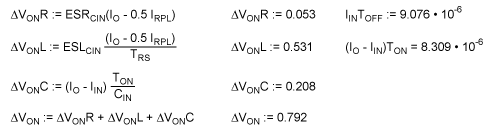
The peak-to-peak ripple is equal to the higher of the two, which is ΔVOFF~1V. As seen from the above, most of the ripple is caused by ESL and the fast di/dt. Di/dt of 1A/nS is very realistic in today's MHz DC-DC converters. Therefore, to reduce the ripple, more capacitors would need to be placed in parallel. Lower value ceramic capacitors, such as 0.1uF in the 0805 or 1206 package, have half the ESL of the 10uF, or ~1.2nH. Place the 0.1uF as close as possible to the sensitive decoupling points.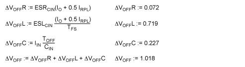
Another parameter that needs to be determined is the RMS current through the input capacitor, so that the capacitor IRMS rating is not exceeded. From the ICIN waveform, the RMS current can be approximated (since the peak-to-peak inductor ripple current is usually 20-30% of IO max) to be:
Where D = (VO + VLS) / (VIN + VLS + VHS), and IIN = (VO × IO) / η × VIN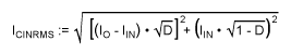
To simplify further, let D = VO/VIN (since V0 >> VLS, and VIN + VLS - VHS ~ VIN), and IIN = VO × IO/VIN (since efficiency η ~ 1), so that the ICINRMS equation above becomes:
The simplified version produces only ~1.4% error, and involves only three known parameters: VI, VO, and IO. VO is fixed, and IO, VI can have a specified range, depending on the application. However, ICINRMS always has a maximum value of IO/2, which happens at VI = 2VO, and decreases the value for VI < 2IO and VI > 2LO. The plot in Figure 2 below illustrates this: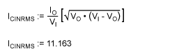
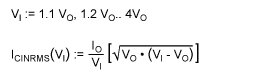
Figure 2.
Due to the high di/dt and pulsating current, a ceramic capacitor is chosen, for its low ESR and ESL. A higher ripple current rating is required at high-frequency to contain the switching spikes. Make sure the RMS current rating of the capacitor is well above the maximum operating RMS current. For long-term reliability, choose a capacitor that will exhibit less than a 10°C temperature rise. Most capacitor manufacturers provide plots that show RMS current vs. temperature rise.
声明:本文内容及配图由入驻作者撰写或者入驻合作网站授权转载。文章观点仅代表作者本人,不代表电子发烧友网立场。文章及其配图仅供工程师学习之用,如有内容侵权或者其他违规问题,请联系本站处理。
举报投诉
-
Mathcad软件实例教程2010-05-04 1325
-
差分阻抗计算的MathCad工作表2008-07-23 3064
-
开关电源设计“利器”Mathcad使用技巧详解2014-11-10 12565
-
Mathcad 14.0 用户手册2016-05-18 580
-
开关电源MATHCAD设计指南2016-06-22 1300
-
MathCAD14.0基础教程2017-02-16 1457
-
mathcad软件资料及应用2017-08-31 1040
-
MathCAD操作指南2017-10-09 1186
-
mathcad学习资料汇编2017-10-09 911
-
MathCAD快速学习手册2021-04-16 1122
-
非常详细的Mathcad - 半桥LLC资料汇总2021-12-06 1774
-
基于Mathcad的LLC公式推导与化简(1)2023-06-23 2817
-
基于Mathcad的LLC公式推导与化简(2)2023-06-23 2247
-
mathcad 在电子和电气工程中的应用2023-12-07 794
全部0条评论

快来发表一下你的评论吧 !
