

Design Guidelines for High-Per
AD技术
10人已加入
描述
Abstract: This application note will help the designer of a high-performance, multichannel, simultaneous-sampling data-acquisition system (DAS). It explains how to select the proper components and place them on the PCB to achieve optimum performance. Maxim's MAX1308, MAX1320, and MAX11046 simultaneous-sampling ADCs are featured. Test data illustrate the benefits of following the guidelines.
The MAX1308, MAX1320, and MAX11046 DAS devices include eight independent simultaneous-sampling input channels and fast successive-approximation ADCs in a single package. To achieve the devices' specifications and to maximize the performance, the designer must take proper care with system architecture, component selection, and PCB layout.
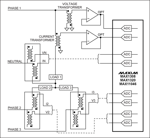
Figure 1. Typical power-grid monitoring application.
Each power phase in Figure 1 is represented by a current transformer (CT) and a voltage transformer (PT). The complete system is comprised of four such pairs (one pair for each of the three phases plus neutral).
By performing digital processing calculations on the simultaneously sampled and digitally converted data, parameters for the instantaneous and average active, reactive, apparent energy, and power factors can be found.
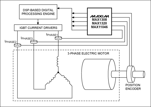
Figure 2. Typical motor-control systems.
Each ADC device in Figure 2 simultaneously samples inputs and eliminates the need for complicated DSP algorithms that realign sequentially sampled data into a simultaneous sample set.
The first class of noise comes from the internal electronic component noise. Sources include ADC conversion process noise and harmonic distortion, buffer amplifier noise and distortions, and reference noise and stability.
A second source of interference is the system's external environment. Examples include external electromagnetic noise, power-supply noise/ripple, I/O pin crosstalk, and digital system noise and interference.
These various noise sources are shown in Figure 3.
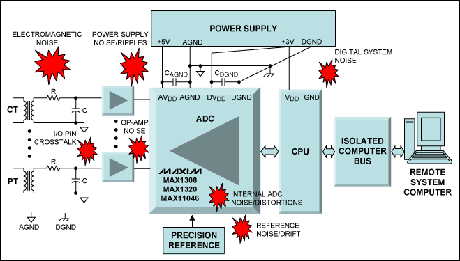
Figure 3. Board-level block diagram of a typical power-line monitoring application. Drawing shows various sources of noise and interference that affect system resolution and accuracy.
A power-line DAS signal-processing chain consists of the CT, PT measurement transformers; anti-aliasing lowpass filters (LPF); buffer amplifiers; simultaneous-sampling ADCs; and the central processing unit (CPU).
A simultaneous-sampling ADC represents the heart of the system; it measures voltages and currents scaled to standard industry input dynamic ranges of +5V, ±5V, or ±10V. Each of the MAX130x, MAX132x, and MAX1104x device families includes derivatives that support these extended ranges without additional signal-conditioning circuits.
Values of 1 LSB and quantization noise for these device families are given in Table 1. These values show the designer what level of total noise and interference is allowed in the DAS, based on the ADC bit numbers.
Table 1. Quantum and Quantization Noise Levels According to the ADC Bit Number
Total noise and ripple in the ADC inputs should be below ½ LSB. At the same time, quantization noise determines the system's ultimate noise floor.
Note: In some designs just 1mVRMS of total noise could ruin the design specification. See Table 2.
Table 2. Example of ADC Resolution Degradation When Total Noise Is Not "Trimmed" Enough
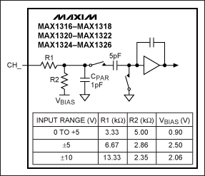
Figure 4. Typical simplified input circuit for the MAX130x and MAX132x families of ADCs.
The main requirements to consider when choosing an amplifier for 12-bit to 16-bit accuracy are: sufficient bandwidth, slew rate, VP-P output, low noise, low distortion, and low offset. Buffer amplifier noise must be kept as low as possible—far below the SNR of the ADC. The amplifier's total offset error, including drift, over the full temperature range should be less than the required accuracy. Each buffer amplifier circuit, therefore, needs to be precisely tailored to the application.
Some recommended high-precision operational amplifiers are shown in Table 3. Some popular op amps are not recommended for high-precision ADCs. See Table 4.
Table 3. Recommended High-Precision Op Amps for Various ADC Resolutions
Table 4. Popular Generic Op Amps Not Recommended for High-Precision ADCs
ZIN = 1/(CIN × FSAMPLE)
Where FSAMPLE is the sampling frequency and CIN = 15pF.
As sampling frequency reduces, input impedance increases:
266kΩ at 250ksps
2.66MΩ at 25ksps
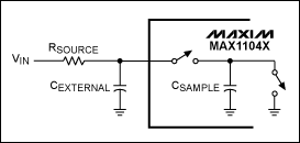
Figure 5. Typical simplified input circuit for the MAX11046 family of devices.
The very high-input impedance values of the MAX11046 family allow direct connection to low-impedance sensors. For example, CT and PT measurement transformers represent relatively low-impedance sensors (in the order of 10Ω to 50Ω) and, therefore, could be connected directly to the MAX11046 inputs using simple lowpass filters.
Table 5 provides the maximum RSOURCE design values for low-frequency applications like power-grid monitoring or motor control.
Table 5. RSOURCE Design Values for CEXTERNAL and FSAMPLE Rates
The correct selection of RSOURCE and CEXTERNAL components is critical to sustaining DAS accuracy.
RSOURCE resistors should be metal film type with 1% or better tolerances and a low temperature coefficient. It is preferable to acquire components from reputable sources like Panasonic®, ROHM®, or Vishay®.
For best results CEXTERNAL capacitors should be ceramic capacitors, and dielectric type COG (NPO) are recommended. These capacitors hold their nominal value over a wide temperature and voltage range. Companies like Kemet®, AVX®, or Samsung® offer a wide selection of cost-efficient SMT parts.
Consider the MAX11046 as an example, where 1 LSB = 62.5µV. The drift specification of the MAX11046's internal reference is ±10ppm/C. Over a 50°C temperature range, the reference could drift as much as ±500ppm or about ±2.048mV (±33 LSB).
In applications where drift is important, an external low-drift reference, such as the MAX6341 (1ppm/C), would be a better choice. A 1ppm/C reference will drift by only 0.2mV over 50°C (or just ±3 LSBs). The MAX6341's reference with an initial accuracy of 4.096 ±0.001 is also much better than the MAX11046's internal reference at 4.096 ±0.0016, thus allowing improved DAS precision and thermal stability.
The MAX11046's reference input current in the external-reference mode is only ±10µA. A serial reference like the MAX6341 with its output current up to 10mA could be used like a single reference with multiple high-performance ADCs, thus eliminating part-to-part reference variations.
Referring to Figure 3, the operating frequency for each CT and PT isolation/measurement transformer is 50Hz/60Hz. In reality, these transformers have a much wider (100kHz) bandwidth and could provide a substantial attenuation/filtering function only in the area of 100kHz and above.
Another main source of noise/interferences comes from the DAS's electronic components located on the PCB. Those components include the CPU and power-supply subsystems. (This is especially true in the case of switching power supplies.) This means that an anti-aliasing and noise-suppression LPF is needed on each input channel of the ADCs. Filter components should also be located as close as possible to ADC inputs. Table 5 above provides some recommended component values for the filters with the MAX11046.
A practical example of these considerations with the MAX11046 is shown in Figure 6. This schematic is implemented as a part of the MAX11046 evaluation (EV) kit. The input schematics for channels 2 through 7 demonstrate a direct connection scheme where an external signal can be directly applied to the ADC without a buffer. Optimal resistors and capacitors for a 10ksps sample rate are found in the Table 5. The values of R = 4.6kΩ and C = 1000pF are an attractive combination for power-line monitoring applications. Channel 0 and Channel 1 in the EV kit can be configured for use with an external buffer, which is needed for applications requiring sample rates of 100ksps or higher. This EV kit can be ordered from the ADC business unit at Maxim®, and it will help to substantially speed up DAS development.
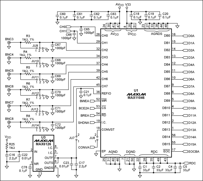
Figure 6. The MAX11046 in a typical connection scheme.
Figure 7. Analog input routing from a connector to the MAX11046.
Note that MAX11046 has very high channel-to-channel isolation. To maintain high isolation, use coplanar strip line structures as shown above.
Precision analog signal form sensors or a signal generator can be connected to the board using the shielded coaxial connectors BNC1 through BNC8. The BNC1 and BNC2 inputs could be configured for direct connect or for use with an external buffer, which is needed for applications requiring sample rates of 100ksps or higher. The BNC3 through BNC8 inputs are intended for direct connect only; external signals can be directly applied to the ADC without a buffer. Simplifying the design without a buffer is why this signal-shielding approach was used for the routing. See Figures 9, 10, and 11.
Implementation of dedicated power planes for analog and digital power distribution is also shown in Figures 11 and 13. The power-plane approach substantially reduces distributed resistance, capacitance, and inductance of the power-line traces and, therefore, improves power and noise efficiency.
Use of the single solid ground plane, with digital signals routed from one direction and analog signals from the other direction, is shown in Figure 12.
More detailed image (PDF, 850kB)
Figure 8. Example of component placement in the 8-channel, MAX11046-based DAS that is available in the EV kit. This view is the silk screen, top.
Figure 9. Example of power-plane partition on the Layer 2 implemented in the 8-channel, MAX11046-based DAS.
Figure 10. Example of signal shield routing implemented on Layer 3 in the 8-channel, MAX11046-based DAS.
Figure 11. Example of the power plane partition on Layer 4 implemented in the 8-channel, MAX11046-based DAS.
Figure 12. Example of a single, solid Layer 5 ground plane with digital signals routed from one direction and analog signals from the other.
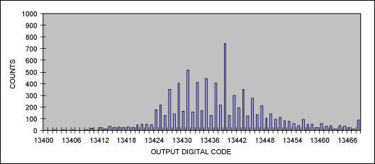
Figure 13. Output histogram for a customer's DAS before improvements were made to the PCB.
Figure 14 is the test results on the customer's prototype PCB after some of the layout improvements discussed in this article were made for power/ground distribution and input signal integrity. Measurements and histograms show a substantial improvement in the DAS's effective number of bits to ~13.5. During this test the histogram patterns became repeatable, reflecting the improved stability of the measurements.
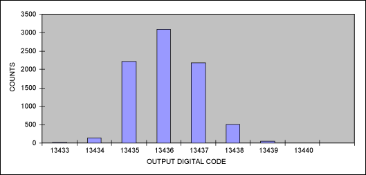
Figure 14. Output histogram for a customer's DAS after improvements for power/ground distribution and signal integrity were made to the PCB.
Figure 15 reflects test results generated on the Maxim DAS in the same industrial lab under similar test conditions. Measurements and histograms show that the DAS's effective number of bits are around 14. During this test the histogram patterns were very repeatable, reflecting the stability of the measurements and the benefits of Maxim's layout and design configuration.
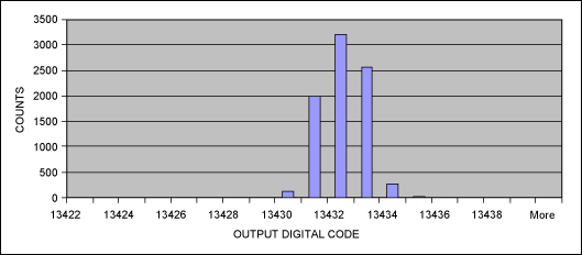
Figure 15. Output histogram for Maxim's DAS.
To achieve the DAS design parameters and to meet the published specifications for these ADCs, special attention is required in critical design areas. Those design considerations involve LPF filters; low-noise buffers and references selection; component placement; PCB layout; and power-supply noise/ripple filtering. With attention to these design principles the newest generation of high-performance ADCs will provide excellent results.
Additional References
Application note 270, "Analog-Signal Data Acquisition in Industrial Automation Systems."
Application note 748, "The ABCs of ADCs: Understanding How ADC Errors Affect System Performance."
Application note 4281, "Advanced Power-Line Monitoring Requires a High-Performance, Simultaneous-Sampling ADC."
打开APP阅读更多精彩内容
Introduction
Many advanced industrial applications require the use of high-performance, simultaneous-sampling, multichannel ADCs. Consider as examples an advanced power-line monitoring (Figure 1) or contemporary three-phase motor-control system (Figure 2). These applications require accurate simultaneous, multichannel measurement over a wide dynamic range of ~70dB to 90dB (depending on the application). A sample rate of 16ksps or higher is common.The MAX1308, MAX1320, and MAX11046 DAS devices include eight independent simultaneous-sampling input channels and fast successive-approximation ADCs in a single package. To achieve the devices' specifications and to maximize the performance, the designer must take proper care with system architecture, component selection, and PCB layout.
Typical Examples of DAS Architecture
Figure 1. Typical power-grid monitoring application.
Each power phase in Figure 1 is represented by a current transformer (CT) and a voltage transformer (PT). The complete system is comprised of four such pairs (one pair for each of the three phases plus neutral).
By performing digital processing calculations on the simultaneously sampled and digitally converted data, parameters for the instantaneous and average active, reactive, apparent energy, and power factors can be found.
Figure 2. Typical motor-control systems.
Each ADC device in Figure 2 simultaneously samples inputs and eliminates the need for complicated DSP algorithms that realign sequentially sampled data into a simultaneous sample set.
Main Sources of Noise and Interference Affecting Industrial Data-Acquisition Systems (DAS)
Two classes of noise/interference can be defined in the DAS.The first class of noise comes from the internal electronic component noise. Sources include ADC conversion process noise and harmonic distortion, buffer amplifier noise and distortions, and reference noise and stability.
A second source of interference is the system's external environment. Examples include external electromagnetic noise, power-supply noise/ripple, I/O pin crosstalk, and digital system noise and interference.
These various noise sources are shown in Figure 3.
Figure 3. Board-level block diagram of a typical power-line monitoring application. Drawing shows various sources of noise and interference that affect system resolution and accuracy.
A power-line DAS signal-processing chain consists of the CT, PT measurement transformers; anti-aliasing lowpass filters (LPF); buffer amplifiers; simultaneous-sampling ADCs; and the central processing unit (CPU).
A simultaneous-sampling ADC represents the heart of the system; it measures voltages and currents scaled to standard industry input dynamic ranges of +5V, ±5V, or ±10V. Each of the MAX130x, MAX132x, and MAX1104x device families includes derivatives that support these extended ranges without additional signal-conditioning circuits.
Values of 1 LSB and quantization noise for these device families are given in Table 1. These values show the designer what level of total noise and interference is allowed in the DAS, based on the ADC bit numbers.
Table 1. Quantum and Quantization Noise Levels According to the ADC Bit Number
| ADC | No. of Channels | No. of Bits | VREF (V) | LSB (mV) | Quantization Noise (mV) |
SNR (dB) |
| MAX1308 | 8 | 12 | 2.5 | 0.6104 | 0.1762 | 71 |
| MAX1320 | 8 | 14 | 2.5 | 0.1526 | 0.0440 | 76 |
| MAX11046 | 8 | 16 | 4.096 | 0.0625 | 0.0180 | 85 |
Total noise and ripple in the ADC inputs should be below ½ LSB. At the same time, quantization noise determines the system's ultimate noise floor.
Note: In some designs just 1mVRMS of total noise could ruin the design specification. See Table 2.
Table 2. Example of ADC Resolution Degradation When Total Noise Is Not "Trimmed" Enough
| ADC | No. of Channels | No. of Bits | No. of Bits Lost at Input Noise (1mV) |
Degraded Resolution |
| MAX1308 | 8 | 12 | 0.71 | 11.3 |
| MAX1320 | 8 | 14 | 2.71 | 11.3 |
| MAX11046 | 8 | 16 | 4.00 | 12.0 |
Electronic Components Selection: DAS Signal-Processing Chain
Choose the Correct Input Buffer Amplifier
The MAX130x and MAX132x families of ADCs have relatively low-impedance input circuitry, as shown in Figure 4. Consequently, in most applications, these devices require an input buffer to achieve 12-bit to 14-bit accuracy.Figure 4. Typical simplified input circuit for the MAX130x and MAX132x families of ADCs.
The main requirements to consider when choosing an amplifier for 12-bit to 16-bit accuracy are: sufficient bandwidth, slew rate, VP-P output, low noise, low distortion, and low offset. Buffer amplifier noise must be kept as low as possible—far below the SNR of the ADC. The amplifier's total offset error, including drift, over the full temperature range should be less than the required accuracy. Each buffer amplifier circuit, therefore, needs to be precisely tailored to the application.
Some recommended high-precision operational amplifiers are shown in Table 3. Some popular op amps are not recommended for high-precision ADCs. See Table 4.
Table 3. Recommended High-Precision Op Amps for Various ADC Resolutions
| Part | Power Supply | Unity Gain Bandwidth (MHz) |
Slew Rate (V/µs) |
VP-P (V) | Offset (mV, max) |
Noise Density (nV/√Hz) |
Comments |
| MAX410–MAX412 | ±5V | 28 | 4.5 | 7.2 | 0.25 | 2.4 | Good for 12 bits to 16 bits |
| MAX4250 | +5V | 3 | 0.3 | 5 | 0.75 | 7.9 | Good for 12 bits to 14 bits |
Table 4. Popular Generic Op Amps Not Recommended for High-Precision ADCs
| Part | Power Supply | Unity Gain Bandwidth (MHz) |
Slew Rate (V/µs) |
VP-P (V) | Offset (mV, max) |
Noise Density (nV/√Hz) |
Comments |
| LF411 | ±15V | 4 | 15 | 20 | 2.0 | 25 | Good below 12 bits |
| LM124 | ±15V | 1.2 | 0.5 | 20 | 3.0 | 35 | Good below 11 bits |
Alternate Input Filter Requirements: MAX11046 Family
The MAX11046 family of devices implements a different input structure that may not require an input buffer amplifier (Figure 5). The MAX11046's effective input impedance, ZIN, is dictated by the input capacitance and sampling frequency:ZIN = 1/(CIN × FSAMPLE)
Where FSAMPLE is the sampling frequency and CIN = 15pF.
As sampling frequency reduces, input impedance increases:
266kΩ at 250ksps
2.66MΩ at 25ksps
Figure 5. Typical simplified input circuit for the MAX11046 family of devices.
The very high-input impedance values of the MAX11046 family allow direct connection to low-impedance sensors. For example, CT and PT measurement transformers represent relatively low-impedance sensors (in the order of 10Ω to 50Ω) and, therefore, could be connected directly to the MAX11046 inputs using simple lowpass filters.
Table 5 provides the maximum RSOURCE design values for low-frequency applications like power-grid monitoring or motor control.
Table 5. RSOURCE Design Values for CEXTERNAL and FSAMPLE Rates
|
| ||||||
| FSAMPLE (ksps) |
0 | 100 | 300 | 1000 | 3000 | |
|
| ||||||
| 1000 | 1.0E+06 | 3.3E+05 | 1.4E+05 | 4.7E+04 | 1.6E+04 | |
| 2500 | 4.0E+05 | 1.3E+05 | 5.7E+04 | 1.9E+04 | 6.5E+03 | |
| 5000 | 2.0E+05 | 6.6E+04 | 2.8E+04 | 9.4E+03 | 3.2E+03 | |
| 10000 | 9.7E+04 | 3.2E+04 | 1.4E+04 | 4.6E+03 | 1.6E+03 | |
| 25000 | 3.7E+04 | 1.2E+04 | 5.3E+03 | 1.8E+03 | 6.1E+02 | |
The correct selection of RSOURCE and CEXTERNAL components is critical to sustaining DAS accuracy.
RSOURCE resistors should be metal film type with 1% or better tolerances and a low temperature coefficient. It is preferable to acquire components from reputable sources like Panasonic®, ROHM®, or Vishay®.
For best results CEXTERNAL capacitors should be ceramic capacitors, and dielectric type COG (NPO) are recommended. These capacitors hold their nominal value over a wide temperature and voltage range. Companies like Kemet®, AVX®, or Samsung® offer a wide selection of cost-efficient SMT parts.
ADC Reference Consideration
Reference selection is also critical to overall DAS performance, and closely related to the required ADC resolution and accuracy. See Table 1 above. Having reasonable drift over the full temperature range and initial accuracy is most important.Consider the MAX11046 as an example, where 1 LSB = 62.5µV. The drift specification of the MAX11046's internal reference is ±10ppm/C. Over a 50°C temperature range, the reference could drift as much as ±500ppm or about ±2.048mV (±33 LSB).
In applications where drift is important, an external low-drift reference, such as the MAX6341 (1ppm/C), would be a better choice. A 1ppm/C reference will drift by only 0.2mV over 50°C (or just ±3 LSBs). The MAX6341's reference with an initial accuracy of 4.096 ±0.001 is also much better than the MAX11046's internal reference at 4.096 ±0.0016, thus allowing improved DAS precision and thermal stability.
The MAX11046's reference input current in the external-reference mode is only ±10µA. A serial reference like the MAX6341 with its output current up to 10mA could be used like a single reference with multiple high-performance ADCs, thus eliminating part-to-part reference variations.
PCB Design and Layout Considerations
Multichannel, simultaneous-sampling ADC design challenges can be discussed in the context of a power-line monitoring application. This presentation will refer to the board-level block-diagram and the main noise/interference sources shown in Figure 3 above.Suppressing Noise—Use a Lowpass Filter (LPF)
The amount of noise/interference present on the power line can be very substantial at any given time. This noise typically arises from the electrical cables/distribution system due to capacitive/inductive coupling with external noise sources. The noise and interference also result from the power line's dynamic nature.Referring to Figure 3, the operating frequency for each CT and PT isolation/measurement transformer is 50Hz/60Hz. In reality, these transformers have a much wider (100kHz) bandwidth and could provide a substantial attenuation/filtering function only in the area of 100kHz and above.
Another main source of noise/interferences comes from the DAS's electronic components located on the PCB. Those components include the CPU and power-supply subsystems. (This is especially true in the case of switching power supplies.) This means that an anti-aliasing and noise-suppression LPF is needed on each input channel of the ADCs. Filter components should also be located as close as possible to ADC inputs. Table 5 above provides some recommended component values for the filters with the MAX11046.
A practical example of these considerations with the MAX11046 is shown in Figure 6. This schematic is implemented as a part of the MAX11046 evaluation (EV) kit. The input schematics for channels 2 through 7 demonstrate a direct connection scheme where an external signal can be directly applied to the ADC without a buffer. Optimal resistors and capacitors for a 10ksps sample rate are found in the Table 5. The values of R = 4.6kΩ and C = 1000pF are an attractive combination for power-line monitoring applications. Channel 0 and Channel 1 in the EV kit can be configured for use with an external buffer, which is needed for applications requiring sample rates of 100ksps or higher. This EV kit can be ordered from the ADC business unit at Maxim®, and it will help to substantially speed up DAS development.
Figure 6. The MAX11046 in a typical connection scheme.
Preserving Signal Integrity with Grounds and Shielding
Input PCB traces which carry sensitive analog signals from the connector to the ADC inputs can be subject to noise, interference, and channel-to-channel crosstalk. Special ground and signal shielding of these analog traces is critical to the integrity of the input signal. Figure 7 shows an example of a PCB layout intended to protect the analog signal.Figure 7. Analog input routing from a connector to the MAX11046.
Note that MAX11046 has very high channel-to-channel isolation. To maintain high isolation, use coplanar strip line structures as shown above.
General PCB Layout Guidelines
Several other important PCB guidelines will help achieve the best performance in multichannel, simultaneous-sampling DAS application.- Use PC boards with ground planes.
- Ensure that the analog and digital lines are separated from each other.
- Do not run digital and analog lines parallel to one another.
- Avoid running digital lines underneath the ADC package.
- Use a single, solid GND plane with digital signals routed from one direction and analog signals from the other.
- Keep the ground return to the power supply for this ground low impedance and as short as possible for noise-free operation.
- Bypass AVDD and DVDD to the ground plane with a 0.1µF ceramic chip capacitor on each pin as close to the device as possible to minimize parasitic inductance.
- Add at least one bulk 10µF decoupling capacitor to AVDD and DVDD for each PC board.
- Interconnect all of the AVDD and DVDD inputs using two solid power planes.
- Bring the AVDD power plane on the analog interface side of the MAX11046 and the DVDD power plane from the digital interface side of the device.
Precision analog signal form sensors or a signal generator can be connected to the board using the shielded coaxial connectors BNC1 through BNC8. The BNC1 and BNC2 inputs could be configured for direct connect or for use with an external buffer, which is needed for applications requiring sample rates of 100ksps or higher. The BNC3 through BNC8 inputs are intended for direct connect only; external signals can be directly applied to the ADC without a buffer. Simplifying the design without a buffer is why this signal-shielding approach was used for the routing. See Figures 9, 10, and 11.
Implementation of dedicated power planes for analog and digital power distribution is also shown in Figures 11 and 13. The power-plane approach substantially reduces distributed resistance, capacitance, and inductance of the power-line traces and, therefore, improves power and noise efficiency.
Use of the single solid ground plane, with digital signals routed from one direction and analog signals from the other direction, is shown in Figure 12.
More detailed image (PDF, 850kB)
Figure 8. Example of component placement in the 8-channel, MAX11046-based DAS that is available in the EV kit. This view is the silk screen, top.
Figure 9. Example of power-plane partition on the Layer 2 implemented in the 8-channel, MAX11046-based DAS.
Figure 10. Example of signal shield routing implemented on Layer 3 in the 8-channel, MAX11046-based DAS.
Figure 11. Example of the power plane partition on Layer 4 implemented in the 8-channel, MAX11046-based DAS.
Figure 12. Example of a single, solid Layer 5 ground plane with digital signals routed from one direction and analog signals from the other.
Test Results
Some test results of the industrial prototype of the MAX11046-based multichip multichannel, simultaneous-sampling DAS are shown in Figures 13, 14, and 15. A precision 2.048V DC reference signal (generated by the MAX6126 voltage reference) was applied to the MAX11046's inputs of the DAS. The ADC output was converted to the range ±32768. Figure 13 is the test results on a customer's prototype PCB that violated many layout guidelines for power distribution and input signal integrity. Measurements and histograms show that the noise/interference reduces the DAS's effective number of bits to ~11.5. During this test histogram patterns were unstable, thus reflecting the unpredictability of the measurements.Figure 13. Output histogram for a customer's DAS before improvements were made to the PCB.
Figure 14 is the test results on the customer's prototype PCB after some of the layout improvements discussed in this article were made for power/ground distribution and input signal integrity. Measurements and histograms show a substantial improvement in the DAS's effective number of bits to ~13.5. During this test the histogram patterns became repeatable, reflecting the improved stability of the measurements.
Figure 14. Output histogram for a customer's DAS after improvements for power/ground distribution and signal integrity were made to the PCB.
Figure 15 reflects test results generated on the Maxim DAS in the same industrial lab under similar test conditions. Measurements and histograms show that the DAS's effective number of bits are around 14. During this test the histogram patterns were very repeatable, reflecting the stability of the measurements and the benefits of Maxim's layout and design configuration.
Figure 15. Output histogram for Maxim's DAS.
Conclusion
High-performance multichannel, simultaneous-sampling ADCs like the MAX1308, MAX1320, and MAX11046 series of devices are especially useful in new DAS applications that must meet or exceed the advanced specifications for the "smart" power grid monitoring (see application note 4281, "Advanced Power-Line Monitoring Requires a High-Performance, Simultaneous-Sampling ADC") or the requirements for contemporary three-phase motor-control systems.To achieve the DAS design parameters and to meet the published specifications for these ADCs, special attention is required in critical design areas. Those design considerations involve LPF filters; low-noise buffers and references selection; component placement; PCB layout; and power-supply noise/ripple filtering. With attention to these design principles the newest generation of high-performance ADCs will provide excellent results.
Additional References
Application note 270, "Analog-Signal Data Acquisition in Industrial Automation Systems."
Application note 748, "The ABCs of ADCs: Understanding How ADC Errors Affect System Performance."
Application note 4281, "Advanced Power-Line Monitoring Requires a High-Performance, Simultaneous-Sampling ADC."
AVX is a registered trademark of AVX Corporation.
Kemet is a registered trademark of KRC Trade Corporation.
Maxim is a registered trademark of Maxim Integrated Products, Inc.
Panasonic is a registered trademark of Matsushita Electric Industrial Co., Ltd.
ROHM is a registered trademark of ROHM Co., Ltd.
Samsung is a registered trademark of Samsung Electronics Co., Ltd.
Vishay is a registered trademark of Vishay Intertechnology, Inc.
声明:本文内容及配图由入驻作者撰写或者入驻合作网站授权转载。文章观点仅代表作者本人,不代表电子发烧友网立场。文章及其配图仅供工程师学习之用,如有内容侵权或者其他违规问题,请联系本站处理。
举报投诉
-
PCIE板设计规则--PCI Express Board Design Guidelines2009-03-26 0
-
Design And Application Guide For High Speed MOSFET Gate Drive Circuits2009-03-27 0
-
PCB设计规范 PCB Design Guidelines Application Note2009-12-09 0
-
EMC Design Guidelines For Electronic Modules2009-12-17 0
-
PCI Express Board Design Guidelines2011-01-28 0
-
Antenna Design and RF Layout Guidelines2017-09-28 0
-
PCB Design Guidelines for SIRF2009-09-20 656
-
Agilent J-BERT N4903B High-Per2010-08-11 592
-
Design Guidelines for High-Per2009-04-16 955
-
Reference Design for a High-Cu2009-05-02 1357
-
Reference Design for a High-In2009-11-08 1168
-
High-Speed_Digital_System_Design2016-02-23 673
-
EE-418: ADSP-2156x Board Design Guidelines for Dynamic Memory Controller2021-01-30 602
全部0条评论

快来发表一下你的评论吧 !
