

Deglitching Techniques for Hig
电源设计应用
419人已加入
描述
In an R-2R DAC design with supply voltages exceeding ±5V, large voltage glitches (up to 1.5V) can occur during the DAC's major-carry transitions. These glitches can propagate through the output buffer amplifier and appear at output. The slewing of the level shifters that control the top (VREF+) and bottom (VREF-) single-pole double-throw switches (S0 to SN) causes the glitches (Figure 1). If each switch of the "inverted" R-2R ladder were turned on and/or off instantaneously, glitch amplitudes at the DAC output (or input of the output buffer amplifier) would be small. However, switches do not switch instantaneously; in fact, to avoid crowbar current between outputs of the two reference buffers, the switches employ a break-before-make connection. The associated time delay can produce very large glitches during DAC code transitions that degrade the dynamic performance specification "glitch impulse energy."
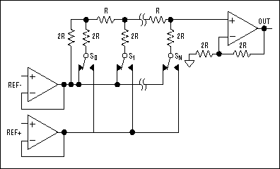
Figure 1. Simplified DAC circuit.
One way to reduce glitch energy is to connect a large capacitor between the DAC output and ground. The lowpass-filter combination of RDAC and C reduces the amplitude of the glitch. However, to reduce the glitch significantly, the capacitance value must be large. Thus, this approach increases the DAC's settling time considerably.
Another deglitching technique is to use an external track/hold (T/H) amplifier following the DAC output. One advantage of this approach is that glitches at the DAC output can be eliminated completely (in principle). However, external one shot and deglitch timing control logic (in addition to the T/H amplifier) are required. Thus, the interface between the DAC, the deglitch timing control circuit, and the T/H amplifier can be fairly cumbersome.
Integrating the T/H amplifier on the same chip as the DAC eliminates the cumbersome interface (Figure 2). The deglitch T/H amplifier is placed immediately following the buffered DAC output. Using this technique, a smart deglitch circuit has been developed that significantly reduces the digital-to-analog glitch impulse energy without increasing settling time.
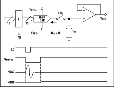
Figure 2. Integrated T/H deglitch architecture.
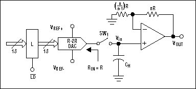
Figure 3. An improved deglitch circuit.
Designating VSW as the switch voltage that controls the sampling switch, the process breakdown voltage (VBREAKDOWN) limits the maximum value of VSW. By setting n>Vout (MIN/MAX)/VBREAKDOWN, the high-voltage concerns are mitigated.
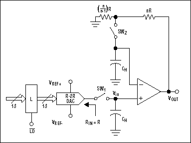
Figure 4. Differential charge cancellation.
SW2 is equal to SW1, and both see the same impedance. The equivalent resistance is equal to R, and the equivalent capacitance is equal to CH.
This architecture improves the circuit performance; however, there are still a few concerns that need to be addressed. First, when SW1 and SW2 are both opened, there is no feedback path for the output amplifier; the amplifier is operating open loop. Second, the hold capacitor at the inverting input of the amplifier can cause additional phase shift, reducing the op amp's phase margin (PM).
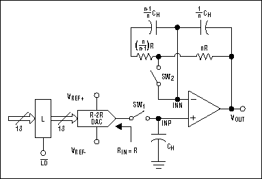
Figure 5. Complete architecture.
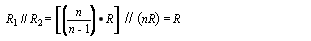
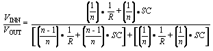
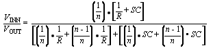
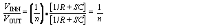
With this configuration, there is no phase shift from VOUT to VINN-. When SW2 opens, C1 and C2 maintain the negative feedback. For the pole-zero cancellation, the equivalent feedback network is shown in Figure 6.
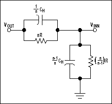
Figure 6. Equivalent circuit of feedback network.
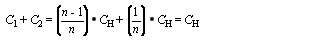
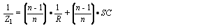
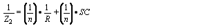
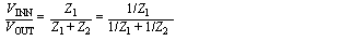
Mathematically, the advantage of this circuit, namely the pole-zero cancellation, is derived as follows:
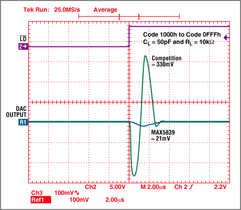
Figure 7. Glitch amplitude during a major-carry transition.
打开APP阅读更多精彩内容
Figure 1. Simplified DAC circuit.
One way to reduce glitch energy is to connect a large capacitor between the DAC output and ground. The lowpass-filter combination of RDAC and C reduces the amplitude of the glitch. However, to reduce the glitch significantly, the capacitance value must be large. Thus, this approach increases the DAC's settling time considerably.
Another deglitching technique is to use an external track/hold (T/H) amplifier following the DAC output. One advantage of this approach is that glitches at the DAC output can be eliminated completely (in principle). However, external one shot and deglitch timing control logic (in addition to the T/H amplifier) are required. Thus, the interface between the DAC, the deglitch timing control circuit, and the T/H amplifier can be fairly cumbersome.
Integrating the T/H amplifier on the same chip as the DAC eliminates the cumbersome interface (Figure 2). The deglitch T/H amplifier is placed immediately following the buffered DAC output. Using this technique, a smart deglitch circuit has been developed that significantly reduces the digital-to-analog glitch impulse energy without increasing settling time.
Figure 2. Integrated T/H deglitch architecture.
Smart DAC Deglitch Circuit
Because the glitch occurs right after a DAC is updated and disappears within the first few microseconds, if the DAC output and output buffer amplifier input are decoupled when the DAC is updated and stay decoupled until the glitch disappears, the glitch will not pass through the output buffer amplifier. As shown in Figure 2, this solution uses a T/H concept to eliminate glitches. Before the DAC is updated, switch SW1 is closed. The sampling capacitor samples the DC level of the previous DAC code. During a digital code transition, as the DAC is being updated the switch is opened and the capacitor (CH) holds the DC level of the previous DAC code. The amplifier output is maintained at this DC level while the glitch occurs. After the glitch disappears, the switch closes again. Unlike the lowpass-filter technique discussed in the previous section, the value of the T/H capacitor can be much smaller, because this capacitor is used to hold the DC level of the previous DAC code, as opposed to reducing the amplitude of a glitch. Small glitches can still occur when the T/H switch is turned on or off due to charge sharing and injection, but the associated glitch amplitude is much smaller.Implementation Techniques
Although combining the DAC output amplifier with a T/H appears obvious intuitively, this presents some design challenges during the actual implementation. For example, in some applications, a large DAC output swing is required. Therefore, the sampling switch (SW1) must operate with high-voltage potentials. This requirement limits the T/H implementation to a handful of processes having the required high breakdown voltage MOS switches. Another challenge is that the base current of the output amplifier's bipolar input pair can cause an offset voltage (IBASE × RSW) across the switch (SW1). Finally, charge injection and clock feedthrough are additional T/H circuit specifications that need to be considered.An Improved Deglitch Circuit
With a unity-gain buffer amplifier following the DAC output, the sampling switch must have a high breakdown voltage. However, if the amplifier's gain is greater than one (n > 1), the required switch breakdown voltage will be reduced by a factor of n. This helps to relax the process requirements as they relate to the DAC and the switch. Figure 3 shows the architecture of this circuit. Figure 3. An improved deglitch circuit.
Designating VSW as the switch voltage that controls the sampling switch, the process breakdown voltage (VBREAKDOWN) limits the maximum value of VSW. By setting n>Vout (MIN/MAX)/VBREAKDOWN, the high-voltage concerns are mitigated.
Eliminating Offset Due to Non-zero Base Current
To eliminate the base current of the sampling switch, differential charge cancellation can be used, as shown in Figure 4. Figure 4. Differential charge cancellation.
SW2 is equal to SW1, and both see the same impedance. The equivalent resistance is equal to R, and the equivalent capacitance is equal to CH.
This architecture improves the circuit performance; however, there are still a few concerns that need to be addressed. First, when SW1 and SW2 are both opened, there is no feedback path for the output amplifier; the amplifier is operating open loop. Second, the hold capacitor at the inverting input of the amplifier can cause additional phase shift, reducing the op amp's phase margin (PM).
Pole-Zero Architecture for the Deglitch Circuit
With a slight change in the amplifier feedback network, the circuit can address the phase-shift problem. As shown in Figure 5, the equivalent impedance at both sides of switches SW1 and SW2 are matched. This circuit effectively adds a zero at the pole location in the amplifier feedback network that compensates for the added phase shift and reduced phase margin of Figure 4. Figure 5. Complete architecture.
With this configuration, there is no phase shift from VOUT to VINN-. When SW2 opens, C1 and C2 maintain the negative feedback. For the pole-zero cancellation, the equivalent feedback network is shown in Figure 6.
Figure 6. Equivalent circuit of feedback network.
Mathematically, the advantage of this circuit, namely the pole-zero cancellation, is derived as follows:
Test Results
This smart deglitch circuit for the voltage DAC technique is currently used in the MAX5839, a 13-bit, octal, high-voltage DAC. Test measurements reveal that the digital-to-analog glitch energy is up to 10 times' smaller than that of other devices on the market. The following plot shows the test results.Figure 7. Glitch amplitude during a major-carry transition.
Conclusions
Using a T/H amplifier technique for deglitch circuits, we achieve very small glitches (typically 10mV to 20mV) at the DAC output during major-carry transitions. By implementing pole-zero cancellation in the RC feedback network, the additional phase shift due to the hold capacitor is eliminated and the stability of the output amplifier is maintained. When the sampling switch is opened, negative feedback is still employed via capacitors C1 and C2. Additionally, base-current cancellation eliminates the voltage offset due to RSW × Ibase. Finally, by properly choosing the gain "n" of the output amplifier, we can use process constraints (which could otherwise complicate the design) to our advantage.
声明:本文内容及配图由入驻作者撰写或者入驻合作网站授权转载。文章观点仅代表作者本人,不代表电子发烧友网立场。文章及其配图仅供工程师学习之用,如有内容侵权或者其他违规问题,请联系本站处理。
举报投诉
-
Impedance Matching Techniques for VLSI Packaging2008-09-10 0
-
PCB design techniques for lowest-cost EMC2009-03-26 0
-
PCB design techniques for lowest-cost EMC compliance2009-03-26 0
-
Synchronous Design Techniques,xilinx同步设计技术2009-06-14 0
-
LabVIEW For Everyone+LabView-Advanced Programming Techniques (2Ed-2007)2011-11-19 0
-
高速PCB设计英文原版(High-Speed_Board_Design_Techniques)2012-10-12 0
-
《LabVIEW—AdvancedProgramming Techniques SECOND EDITION》2015-03-20 0
-
求一本Mathematical Techniques in Multisensor Data Fusion2021-06-22 0
-
Computational Techniques for V2008-11-03 410
-
PCB design techniques for lowe2009-03-24 444
-
Computational Techniques for Voltage Stability Assessment an2009-07-21 360
-
Advanced DSP Design Techniques2010-07-01 304
-
Jitter Analysis Techniques Usi2010-07-19 377
-
Equalizing Techniques Flatten2009-02-21 791
全部0条评论

快来发表一下你的评论吧 !
