

900MHz全双工无线发射器参考设计,Transmitter
通信设计应用
描述
900MHz全双工无线发射器参考设计,Transmitter Reference Design for a 900MHz Full-Duplex Radio
Abstract: This reference design covers the design of a transmitter inside a 900MHz full-duplex radio using the MAX2902 single-chip transmitter. The MAX2902 is designed for use in the 869MHz to 915MHz frequency band, and complies with FCC CFR47 part 15.247 902MHz to 928MHz ISM band specifications. The reference design is capable of delivering more than +19dBm with VCC = 2.9V and ICC = 170mA, and +20dBm with VCC = 3.3V and ICC = 190mA, while meeting 14dB of CNR (1.22Mbps BPSK) at 10:1 VSWR (all angles).
Figure 1. Reference design board features the MAX2902 single-chip transmitter, which is designed for use in 868MHz to 915MHz frequency band. The device complies with FC CFR47 part 15.247 902MHz to 928MHz ISM band specifications. 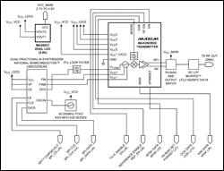
More detailed image (PDF, 213kB)
Figure 2. Reference design block diagram for the MAX2902 900MHz BPSK transmitter. Shows characterization report (v1b), block diagram, and interface connects. Dedicated LDO for Tx IC VCO and TCXO is to mitigate coupling from PA. The second LDO output supplies the synthesizer and the Tx IC (all but the PA). The transmitter's PA is supplied directly by the system (VCC_MAIN). An additional PA is required to get > 18dBm output power while meeting 20% EVM requirement at 8:1 VSWR. The 40MHz WLAN TCXO was used as a temporary replacement for the intended 16.36MHz GPS reference originally specified. The PLL can accommodate any common reference frequency from 1MHz to 50MHz. The customer should select their TCXO based on cost and tolerance for phase noise of the unmodulated carrier.
| Lab Measurements |
System Performance Summary
Measured at ANT RF SMA; VCC = 3.3V; TA = +25°C; REF-OSC Freq = 40MHz; PLL locked at 900MHz; LDOEN = high; CSB = high; SCLK = DIN = Low; 2.5VP-P 1.0Mbps PN bit stream (unfiltered) applied to BPSK input, unless otherwise noted.
| Parameter | Conditions and Comments | Target | Measured | Units | ||
| Supply Current | Shutdown mode (LDOEN = LOW), VCC = 4.5V (worst case) | 1.7 | µA | |||
| For +17.5dBm at LPF output (VASK = 2.1) Includes LMX2353 synthesizer and TCXO supply current. |
141 | 104 | mA | |||
| Tuning Range | Range of VCO, freq determined by PLL | 902 to 928 | 902 to 928 | MHz | ||
| LO Integrated Phase Error | In 2MHz BW of demodulator, no modulation | 1.6 | °RMS | |||
| Phase EVM | EVM contribution from the above RMS phase error (for small angles, approximate EVM by ΦERR/(360/2pi) |
2.8 | % | |||
| Magnitude EVM | No modulation | 0.2 | % | |||
| 1.0Mbps PN sequence BPSK modulation | 13 to 14 | % | ||||
| Full-Power EVM | VASK = 2.1V, 8:1 VSWR (worst-case angle) Dominated by distortion due to VCO pulling |
VCC_MAIN = 2.7V, ICC = 106mA (50Ω pwr = +16.9dBm) | 20 | 40.2 | % | |
| VCC_MAIN = 3.3V, ICC = 114mA (50Ω pwr = +19.2dBm) | 20 | 43.6 | ||||
| VCC_MAIN = 4.0V, ICC = 138mA (50Ω pwr = +20.6dBm) | 20 | 53.3 | ||||
| VCC_MAIN = 4.5V, ICC = 299mA (50Ω pwr = +21.3dBm) | 20 | 30.1 | ||||
| Output Power | 50Ω load, 1.0Mbps BPSK modulation (Power at balun output is approx 1dB higher, due to BPF, T-line, SMA) EVM for specified VSWR (worst-case phase angle) is less than 20% |
VASK = 2.1V (for 1:1 VSWR tolerance) |
VCC_MAIN = 2.7V, ICC = 103mA | 16.9 | dBm | |
| VCC_MAIN = 3.3V, ICC = 133mA | 17.5 | 19.2 | ||||
| VCC_MAIN = 4.0V, ICC = 141mA | 20.6 | |||||
| VCC_MAIN = 4.5V, ICC = 145mA | 21.3 | |||||
| VASK = 1.7V (for 4:1 VSWR tolerance) |
VCC_MAIN = 2.7V, ICC = 103mA | 16.7 | ||||
| VCC_MAIN = 3.3V, ICC = 108mA | 18.2 | |||||
| VCC_MAIN = 4.0V, ICC = 112mA | 19.0 | |||||
| VCC_MAIN = 4.5V, ICC = 114mA | 19.4 | |||||
| VASK = 1.6V (for 8:1 VSWR tolerance) |
VCC_MAIN = 2.7V, ICC = 95mA | 16.2 | ||||
| VCC_MAIN = 3.3V, ICC = 99mA | 17.2 | |||||
| VCC_MAIN = 4.0V, ICC = 102mA | 17.8 | |||||
| VCC_MAIN = 4.5V, ICC = 104mA | 18.1 | |||||
| Reference Spurs | fCOMP = 2MHz, worst-case condition: VCC = 4.5V, +21.3dBm output power Actual measurement was < -63dBc (below noise floor of VSA) |
< -41 | < -42 | dBm/MHz | ||
| Output Harmonics | 2nd harmonic levels, at LPF output (limit is -27dBm/MHz in nonrestricted bands) | < -30 | -42 | dBm/MHz | ||
| 3rd harmonic levels, at LPF output (limit is -41dBm/MHz in restricted bands) | < -49 | -54 | ||||
| Measurement Data |
More detailed image (PDF, 222kB)
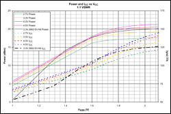
Figure 3. Output power and supply current at various supply voltages as a function of PA gain (VASK).
Note that the reference design incorporates a 900MHz BPF (approx. 0.6dB IL) at Tx output. Reference design and EV kit provide almost identical output power at the PA.
Supply current for the reference design is less than 10mA higher than the EV kit at full power. This is due to the increased bias to the PA that decreases the VCO pulling.
More detailed image (PDF, 219kB)
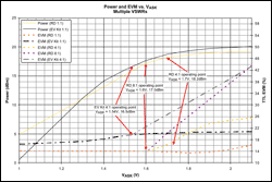
Figure 4. Output power and EVM at various VSWRs, as a function of PA gain (VASK).
Recommended operating points reflect VASK levels to keep EVM below 20% at a desired max VSWR (worst-case phase).
Reference design allows a higher nominal output power for same EVM.
More detailed image (PDF, 218kB)
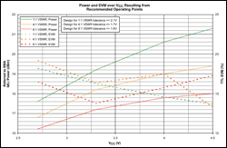
Figure 5. Output power and EVM at various VSWRs as a function of VCC.
VASK is optimized in the design according to the worst-case VSWR the system can tolerate. Lowering VASK drops POUT, but keeps EVM in check for increasing VSWR. Use the following VASK settings to limit EVM to 20%:
Design for 1:1 VSWR tolerance ≥ 2.1V
Design for 4:1 VSWR tolerance ≥ 1.7V
Design for 8:1 VSWR tolerance ≥ 1.6V
| Detailed Description |
The MAX2902 is single-chip transmitter designed for use in 868MHz to 915MHz frequency bands. It complies with FC CFR47 part 15.247 902MHz to 928MHz ISM band specifications.
The transmitter IC offers a high level of integration while minimizing external components. The transmit modulator, power amplifier, RF VCO, 8-channel frequency synthesizer, and baseband PN sequence lowpass filter are all integrated. By filtering BPSK modulation, the spurious emissions are reduced, enabling up to 8 independent transmit channels in the U.S. ISM band. Inputs are provided for spread-spectrum BPSK, ASK, and OOK. FM can be achieved by directly modulating the VCO. The device is intended primarily for use with external differential antenna.
In this reference design the MAX2902 is applied as the transmit IC in the 900MHz band. It is controlled by a National Semiconductor LMX2353 fractional-N PLL.
- 相关推荐
- 无线发射
-
设计一个无线发射器的PCB小凡 2022-09-14
-
无线全双工通信2013-04-11 0
-
HOLTEK:基于HT66FW2230开发Qi无线充电发射器2015-01-29 0
-
全双工无线系统的实现2019-07-11 0
-
UHF频段RFID系统与900MHz无线网络的电磁兼容性分析2021-05-31 0
-
关于发布800/900MHz 频段射频识别(RFID)技术应2009-12-11 515
-
Transmitter Reference Design f2008-08-18 938
-
FM跟踪发射器FM Tracking Transmitter2009-12-22 2425
-
激光发射器/接收器电路 LASER Transmitter/2010-02-05 5489
-
爱立信华为交锋非洲首个900MHz 3G网络2010-03-10 730
-
全双工,全双工是什么意思2010-03-17 4167
-
900MHZ低噪声放大器电路2010-10-31 2797
-
基于MAX2902全双工无线电中的发射机设计2021-04-17 2266
-
声表面波900MHz产品规格批准单2021-06-30 396
-
中国联通获批重耕900MHz2022-11-13 2135
全部0条评论

快来发表一下你的评论吧 !
