

Sequencing Circuit Provides Ps
电源设计应用
描述
Sequencing Circuit Provides Pseudo Voltage Tracker
Abstract: This application note presents three approaches to track voltages between the supply rails. The featured circuit, also the simplest approach, features the MAX6819 power-supply sequencer which performs open-loop voltage tracking.
This design idea appeared in the June 1, 2006 issue of Portable Design magazine.
Modern microcontrollers, DSPs, and ASICs require multiple supply voltages for proper operation. With higher speed and better processing capabilities, the voltages and fabrication geometries of these devices have been scaled down to minimize power dissipation and die space. Many digital ICs are, therefore, susceptible to internal breakdown, if the absolute value of the differential voltage between the supply rails exceeds a specified tolerance during power-up or power-down. The resulting stress can damage the IC immediately, or it can introduce a reliability issue by remaining latent until a later date.
Various voltage-tracking techniques can eliminate this problem. For example, the system can control tracking at the power supply by measuring and actively matching the voltage-versus-time profile of each power rail (Figure 1a). In another closed-loop approach, a shunt architecture (Figure 1b) temporarily shorts the supply rails together during power-up and power-down. The shunt approach reduces power loss across the MOSFET during normal operation, when the MOSFET is off.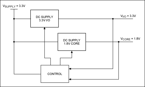
Figure 1a. This voltage-tracking architecture controls the feedback of independent DC/DC regulators. Note: The name of these terminals, and the way the control block adjusts the output voltages, depends on circuitry internal to the power supplies.
Figure 1b. This closed-loop shunt architecture for voltage tracking reduces power loss. Here the MAX5035 DC-DC converter serves as tracking controller.
A simpler, open-loop tracker may be adequate in some cases. A power-supply sequencer circuit (IC1, the MAX6819, in Figure 2) can be configured to perform the voltage-tracking function. Unlike the closed-loop methods, this approach does not short out the power rails or require the control of a DC/DC regulator's feedback loop.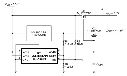
Figure 2. A voltage sequencer (the MAX6819) forces the core and I/O voltages to track by controlling the n-channel MOSFETs simultaneously.
The core and I/O supply voltages are off when the MOSFETs are off (Figure 2). Then, as the voltage monitored at SETV exceeds its threshold, an internal charge pump generates a voltage (GATE output) that enhances the gates of the n-channel MOSFETs simultaneously. If the drain voltages of these two switches are within a few volts of each other, and if the drain currents are not too dissimilar, then the VI/O and VCORE voltages ramp up together as their common gate voltage rises (Figure 3). The differential between the rails is about 200mV, caused by a slight difference in gate turn-on voltages for the FETs used. To increase the ramp time, you can add a small capacitor at the GATE output (COPT) to decrease the slew rate.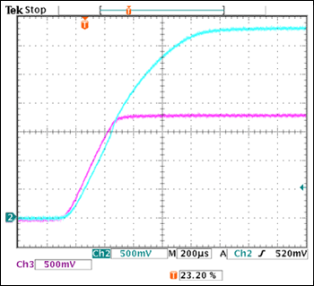
Figure 3. This scope photo illustrates the tracking of VI/O (upper trace) and VCORE in the circuit of Figure 2, where VI/O = 3.3V, VCORE = 1.8V, and both loads are adjusted to 1A.
The Figure 2 circuit can also monitor the supply voltages. If the 3.3V rail falls below about 2V, or if the 1.8V rail falls below the threshold set by the R1/R2 voltage-divider, the GATE output goes low and turns off both MOSFETs. Resistors R1 and R2 determine the actual shutoff level. (The values shown monitor the 1.8V rail.) You can turn off the circuit by pulling the enable input (EN) low.
As a bonus, the circuit automatically "retries" after responding to a shorted load. If the short appears to the right of the dotted line ("A" in Figure 2), the collapse of either or both supplies opens the switches and disconnects both loads from the supply voltages. The formerly shorted power rail returns, and a 200ms delay built into the MAX6819 again closes the switches to test the load after the delay. This load testing continues at 200ms intervals until the short disappears or until the supplies are turned off.
- 相关推荐
- Voltage
-
ps入门到精通,小白也能学会的Photoshop教程-1-PS导学视频电子学习 2023-01-07
-
Design of Combinational Circuit2008-09-11 0
-
Diode Circuit2009-08-20 0
-
PS810 pdf datasheet2008-08-11 749
-
PS4160EV pdf datasheet2008-08-14 1194
-
PS2070 pdf datasheet2008-08-14 574
-
Microwave Solid State Circuit2008-12-23 601
-
Simple Circuit Protects System2009-04-17 527
-
Handy Circuit Gives Systems Fl2009-04-29 1473
-
简单的电路保护系统过热-Simple Circuit Pro2009-05-04 557
-
实现电池反接保护的电路, Circuit Provides2009-07-18 2123
-
Sequencing with the MAX16046 S2009-11-16 1223
全部0条评论

快来发表一下你的评论吧 !
