

浅谈集成FPGA的两种方式:eFPGA(SoC)& cFPGA(SiP)
描述
FPGA is widely popular in systems for its flexibility and adaptability. Increasingly, it is being used in high volume applications. As volumes grow, system designers can consider integration of the FPGA into an SoC to reduce cost, reduce power and/or improve performance.
FPGA以其强大的灵活性和适应性见长。系统设计师在设计大容量复杂应用时,越来越多的考虑使用SoC中集成FPGA方案来减小功耗并提高性能。
There are two options for integrating FPGA into an SoC:o FPGA chiplets, which replace the power hungry SERDES/PHYs with special die-to-die interconnects to communicate with the companion SoC dieo eFPGA, which is an IP block that is put on the SoC dieHow do these alternatives compare? As we’ll see, it depends on the application and the priorities.
There are several applications where integrating an FPGA has advantages:1.In an existing system where an FPGA is paired with an SoC, for example a Smart NIC or Microsoft Azure2.To provide flexibility for an SoC to change algorithms and/or protocols as standards change or for the needs of different customers3.Acceleration for SoCs where critical workloads run faster on parallel FPGA than processors4.To provide programmable state machines in architectures that have arrays of compute elements, such as many new AI accelerators
将FPGA集成进SoC的好处显而易见:1.对于已有的FPGA SoC系统,例如SmartNIC智能网卡方案或者微软Azure云中,可以进一步提高集成度和性能。2.让原本不具备灵活性的SoC具备一定的可编程能力,让终端用户可以根据需求的变化修改协议和算法。3.给SoC提供一个加速核,把一些适合FPGA并行计算的工作负载offload到FPGA上进行。4.在SoC架构中提供可编程状态机等计算单元,作为新型AI引擎总而言之一句话,FPGA具备的好处,SoC集成后可以全部继承。
eFPGA(SoC) & cFPGA(SiP)
目前流行的两种集成方案分别是embedded FPGA(以下简称eFPGA集成方案)以及FPGA Chiplets(以下简称cFPGA集成方案)1.eFPGA集成方案eFPGA是嵌入到SoC中的FPGA IP核,可以是软核或者是硬核,工艺节点往往需要和SoC保持一致。
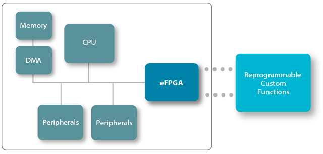
eFPGA的框架(来自QuickLogic)
eFPGA的概念(来自Achronix)
eFPGA通常具有比传统FPGA更多的输入和输出,可连接到总线、数据路径、控制路径、PHY等部件中。这个技术多年前在学术界就已被提出,直到近5年才逐步被广泛接受,美国、法国、中国也涌现了一系列专注于eFPGA的公司,并将其成功的商业化。cFPGA集成方案Chiplet的概念则最早来自 DARPA 的 CHIPS(Common Heterogeneous Integration and IP Reuse Strategies)项目。是通过die-to-die内部互联技术将多个模块芯片与底层基础芯片封装在一起,构成多功能的异构System in Package(SiP)芯片的模式。理论上讲,这种技术是一种短周期、低成本的集成第三方芯片(例如I/O、存储芯片、NPU等)的技术,各个模块芯片的工艺节点可以不同。Chiplet是业界为了弥补硅工艺技术增长放缓所做的几项努力之一。它们起源于多芯片模块,诞生于20世纪70年代,迄今为止,已经有很多公司早早地创建了自己的 Chiplet 生态系统,包括Marvell、AMD、Intel等。
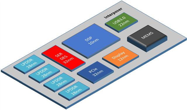
Chiplet的框架
Chiplet的概念
The power-hungry high speed SERDES are the connectivity tiles in this diagram. EMIB is Intel’s proprietary wide-bus high bandwidth chip-to-chip interconnect.The FPGA chiplet in the middle is primarily digital logic. Intel and Xilinx will, for certain customers at least, provide die for integration into SoCs using interposers, see an example below:
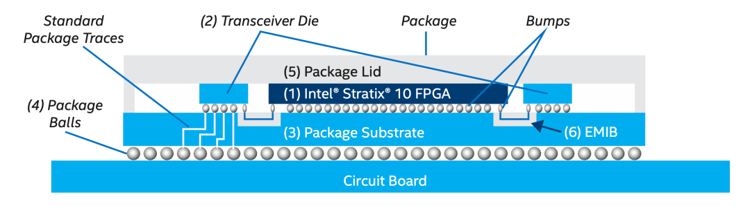
Intel 片间互连技术方案(来自Intel)In this way, an SoC and an FPGA chiplet can be co-packaged with a wide, high speed bus connecting them.最新型的FPGA(无论是X家还是I家),实际上都使用了Chiplet技术。Intel给自家的片间互连技术起了一个高大上的名字:“嵌入式多片互连桥接,Embedded Multi-die Interconnect Bridge”EMIB (如上图所示),其混合了SoC和SiP技术。Xilinx则从7系开始就采用了片间互连技术来在有限的面积下通过堆叠实现超大逻辑容量、Serdes高速接口以及HBM高带宽存储的融合。
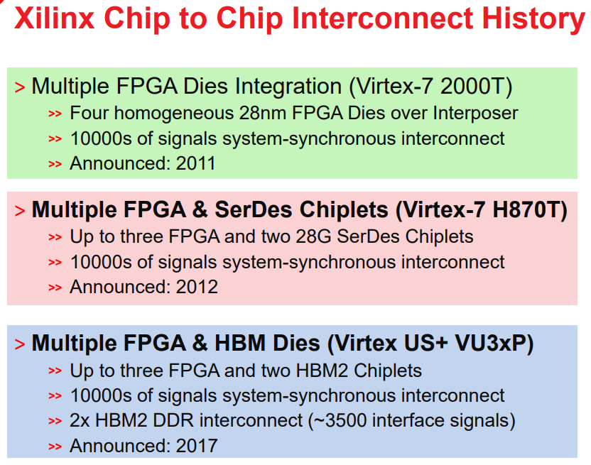
Xilinx 片间互连技术历史(来自Xilinx)
Pros and cons of cFPGA vs eFPGA
两种方案的优劣对比(由于原文作者是FlexLogix的CEO,因此文章也倾向性地强调了eFPGA的好处)
The disadvantages of the chiplet approach are:o the high cost of multi-die packaging using substrateso the need to use a specialized die-to-die interface on your SoC that you may not be familiar with or are unable to get from your PHY IP suppliero the smallest FPGA chiplets available still have a large number of LUTs which may exceed the requirementThe applications where eFPGA may be a better solution are:o those where the die cost of eFPGA+SoC is lower than the cost of the interposer and chiplet+SoCo those where the amount of eFPGA required is 10s of thousands of LUTs: such small chiplets are not available and the die area required on the SoC is minimalo architectures where eFPGA is distributed across the die in many locations, such as in an array of compute elements where the eFPGA is a programmable state machine for local control of high speed compute blocks: chiplets are really only practical for a single large block of FPGA
cFPGA SiP方案的优势:
1.支持多工艺节点的片间融合。
2.旨在打造标准化、模块化的IP,因此FPGA部分通常是一个固定芯片模块,SiP设计的重构迭代速度更快。
eFPGA SoC方案的优势:
1.无需去了解你可能并不熟悉的SoC片间互连技术(有时无法从你的PHY IP提供商那获得)。
2.免去了高昂的多片封装基板费用。
3.旨在强化FPGA的可定制性,在个性化细节定制方面更加灵活。
编辑:hfy
-
Achronix宣布其Speedcore eFPGA IP核出货量超千万个2021-03-26 1925
-
关于eFPGA性能分析和SoC架构师的分析介绍2019-09-15 776
-
掌握这几步充分发挥eFPGA性能,SoC架构师都懂的选型技巧2019-07-04 0
-
求大神分享基于FPGA的DDFS与DDWS的两种实现方式2021-04-30 0
-
嵌入式 FPGA (eFPGA) 时代已到!浅谈FPGA技术的过去、现在和未来2021-11-09 0
-
如何使用寄存器级读&写控制基于PXI平台的FPGA2017-10-19 583
-
可编程硬件发展路线分析:eFPGA还是FPGA SoC2018-02-10 2800
-
一文读懂eFPGA 选择是要注意的四个步骤2018-06-29 2122
-
SoC设计中嵌入FPGA(eFPGA)内核实用评估方法2018-09-20 3873
-
Achronix出席D&R IP SoC China会议,介绍并展示Speedcore eFPGA如何加速边缘计算2018-09-27 4051
-
关于MPU, FPGA SoC以及eFPGA2019-01-17 5632
-
eFPGA是什么?几个关于eFPGA的常见迷思2019-01-27 8570
-
对于eFPGA该如何选择2019-07-29 591
-
对于eFPGA与FPGA SoC之间的对比分析和异同2019-09-04 3655
-
Achronix Speedcore eFPGA IP性能介绍2022-12-23 300
全部0条评论

快来发表一下你的评论吧 !
