

Avoid overvoltage stresses by
模拟技术
描述
Avoid overvoltage stresses by minimizing power-supply pumping on single-ended output, Class D audio amplifiers
Abstract: This application note explains what power-supply pumping is and how it occurs in designs that employ a Class D audio amplifier with single-ended output loads. The article presents three design solutions that will reduce the problem. Mathematical equations show that use of power-supply capacitors greater than 1000µF greatly reduce the phenomenon. The MAX9742 Class D amplifier serves as design example.
This app note is based on a similar article that was published in April 2009 on the Planet Analog website.
Introduction
A strange phenomenon can occur with Class D audio amplifiers that have single-ended output loads: the power-supply voltage increases as power is delivered to the load. The phenomenon is known as power-supply "pumping," and an engineer unfamiliar with Class D amplifiers may find it very puzzling. If the power-supply pumping is not remedied, the voltage increase in the power supply can damage the system.
This application note discusses the causes of power-supply pumping and presents solutions to address it. The MAX9742 Class D amplifier serves as the example circuit.
Understanding power-supply pumping
Power-supply pumping typically occurs when outputting low-frequency waveforms into low-impedance loads. Many power supplies can only source current from the positive output and sink current from the negative output. However, most laboratory power supplies or linear power supplies are rectified with diodes, and thus not designed to sink current from the positive output and source current from the negative output.
Figure 1 shows a typical power supply connected to the MAX9742. When the output at the speaker swings below ground for the negative cycle of the sinewave, current flows into the output through the paths shown by the arrows. Since the MAX9742 is a Class D amplifier, the output at node A swings from VDD to VSS. MOSFET M1 turns on to pull the voltage of node A up to VDD, and MOSFET M2 turns on to pull the voltage of node A down to VSS. The currents shown by the arrows alternate, depending on whether M1 or M2 is on. With M2 on, the current flows through M2 and then returns to the power supply through D2. With M1 on, the current flows through M1, and D1 gets reverse biased so the current is dumped into C1. This current, in turn, increases the magnitude of the voltage at VDD.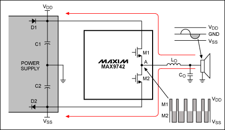
Figure 1. Illustration of the current flow into the outputs during the negative cycle of the sinewave.
Figure 2 shows the power-supply waveform and speaker-output waveform that would occur during power-supply pumping. The waveform from t1 to t2 represents the negative half cycle, which is similar to the current direction in Figure 1. It can be seen that VDD (Channel 1 in yellow) is pumped to a more positive voltage between t1 and t2. As the output sinewave changes to the positive cycle at t2, the increased voltage on VDD is discharged from C1. At the same time, VSS (Channel 2 in blue) becomes more negative as charge is dumped into C2 due to the increasing positive output voltage. The cycle will repeat itself when the output waveform begins to swing negative again.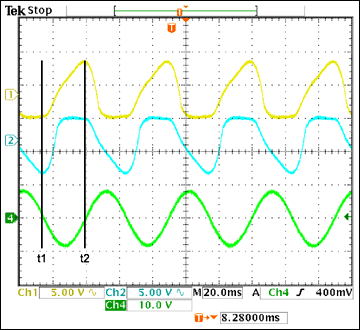
Figure 2. Illustration of the effects of power-supply pumping. The time from t1 to t2 represents the negative half cycle of the output waveform.
The Figure 2 data are from one of the MAX9742's outputs. VDD and VSS were ±15V and 1000µF capacitors were placed on both power supplies. The output was loaded with 4Ω resistors and the input signal was 20Hz.
Power-supply pumping is a bigger problem during low-frequency operation because the power supply is pumped for a longer period during low frequencies, that is, before an opposite phase waveform is output to discharge the power supply capacitors C1 or C2.
Power-supply pumping can cause the application to exceed absolute maximum ratings, thus potentially damaging the capacitors C1 and C2 and/or the output MOSFETs M1 and M2 inside the MAX9742 or other Class D amplifier.
Solutions for power-supply pumping
There are three simple methods to reduce the problem.
- Since the MAX9742 has two single-ended outputs, you can bridge both outputs to become one channel. In a bridged-output configuration, the outputs signals are out of phase with respect to each other. Thus the power-supply pumping in one channel will cancel the pumping in the other channel.
- In most audio tracks, the low-frequency energy in the music is mono (i.e., the same for the left and the right channels). Therefore, one can reverse the polarities of Channel 2 with respect to Channel 1. As shown in Figure 3, the audio input on Channel 2 is inverted. The Channel 1 and Channel 2 outputs are out of phase with respect to each other, so the power-supply pumping that occurs in one channel cancels the pumping in the other channel. In this case the audio connection at the speaker terminals on Channel 2 need to be connected in opposite polarity. This configuration will "un-invert" the output signal of Channel 2 so that the audio content of Channel 1 and Channel 2 are now in phase with each other.
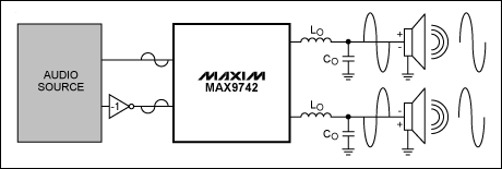
Figure 3. Illustration shows how to reverse the polarities of Channels 2 and 1 to overcome power-supply pumping.
- Larger power-supply capacitors (< 1000µF) also help reduce the magnitude of the power-supply pumping. The larger capacitors accept more current before the power supply gets "pumped up." While the capacitors are receiving the current, there is more time for the opposite phase signal to discharge the pumped supply voltage.
Mathematical model
A good approximation for power-supply pumping can be modeled using equation 1:
For simplification we assume:
VDD = VSS
RDS(ON) for M1 and M2 = 0
Therefore:
| ΔVDD = (1/C) × (A/RLOAD) × [(1/2 × π) - (A/8VDD)] × TSINE | (Eq. 1) |
Where:
C is the bypass filter capacitor on the VDD supply (C1)
A is the amplitude of the output sine wave
RLOAD is the speaker impedance
VDD is the nominal positive supply-voltage value
TSINE is the period of the output sine wave
Equation 1 is for a parabola where the peak of the waveform occurs when the amplitude A = (2/π) × VDD.
Using A = (2/π) × VDD and plugging into equation 1, we obtain the maximum power-supply pumping voltage:
| ΔVDD(max) = [VDD/(2 × π × π)] × [TSINE/(RLOAD × C)] | (Eq. 2) |
In a ±15V power supply and for 8Ω speaker loads with a 20Hz sinewave output, VDD could pump up to 21.6V with 220µF power-supply capacitors. Increasing the size of the power-supply capacitors to 1000µF would reduce this maximum supply pumping voltage to 4.7V. Equation 2 thus shows that the power-supply pumping voltage can be reduced if the design uses power-supply capacitors greater than 1000µF.
文章来源:http://www.elecfans.com/article/analog/2010/20100418216214.html
Conclusion
Power-supply pumping is a problem that occurs when playing low-frequency audio signals through a single-ended output, Class D amplifier driving a low-impedance load. Although power-supply pumping can be troublesome, by understanding this phenomenon and applying the solutions presented here, the problem can be easily reduced to a safe level for both the amplifier and external components.
- 相关推荐
- D类
-
Solid State Overvoltage Protector for AC Line2009-05-12 0
-
MAX6495 pdf datasheet (72V,Overvoltage-Protection Switches/Limiter Controllers)2009-01-11 1102
-
NCP346 Overvoltage Protection2009-11-26 390
-
TPS2400,pdf(Overvoltage Protec2010-10-28 423
-
Flexible overvoltage/undervolt2010-12-12 837
-
LTC4367: 100V Overvoltage, Undervoltage and Reverse Supply Protection Controller Data Sheet2021-01-29 442
全部0条评论

快来发表一下你的评论吧 !
