

The quick guide to layout cons
电源设计应用
419人已加入
描述
This application note describes basic layout guidelines for a Li+ battery charger simulator.
As seen in Figure 1, the major power path of the simulator circuit begins at the BATT+ node, flows through the 100mΩ series input resistance and the TIP35 transistor, and returns at the BATT- node.
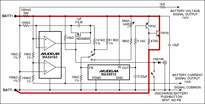
Figure 1. "Charge" current path in the Li+ battery-charger simulator.
Assuming a 3A charge current, the input sense resistor must handle at least 900mW. To ensure a constant input series resistance during operation, use a resistor capable of handling more than 1W. A single 5W resistor or multiple 1W resistors in parallel work well.
The TIP35 transistor handles the bulk of the power through the circuit in both point-by-point mode and integrating mode. Under the worst-case conditions, power across the TIP35 transistor can be calculated as:
Figures 2 and 3 show a sample layout for a 2-layer board. Figure 2 also shows the component labels for the layout in Figures 3A, 3B, and 3C. The board is set up to use multiple sense resistors (up to five) in parallel for the input series resistance; it also allows a second capacitor across the NDS0605 MOSFET. (We used two 0.047µF capacitors here). Although not shown in the figures, use vias between BATT- and the bottom layer for better ground connections. Figure 3 shows the component placement on both layers of the board.
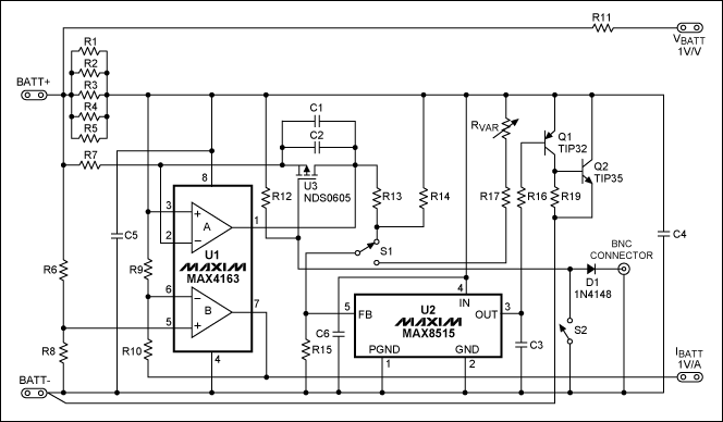
Figure 2. Li+ Battery simulator layout for a 2-layer board.
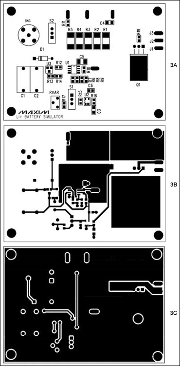
Figure 3. Component placement on the board. Component reference numbers in Figures 3A, 3B, and 3C are shown in the layout of Figure 2. Figure 3A. Li+ battery simulator circuit, 2-layer board, component placement. Figure 3B. Li+ battery simulator circuit, 2-layer board, top layer. Figure 3C. Li+ battery simulator circuit, 2-layer board, bottom layer.
The TIP35 transistor is connected to the circuit at the edge of the board and is connected externally to a large copper heatsink (Figure 4). Thermal paste has been used to enhance the connection between the transistor and the heatsink.
More detailed image (PDF, 916kB)
Figure 4. Li+ battery simulator with external heatsink.
打开APP阅读更多精彩内容
Introduction
Maxim describes a lithium-ion (Li+) battery simulator circuit in application note 4322, "Simplified lithium-ion (Li+) battery-charger testing." While Maxim does not sell evaluation (EV) boards for this circuit, the Company has received multiple requests for one. Responding to customer interest, this application note provides some basic layout guidelines and considerations for designing your own board.Test board for the battery simulator
Making a board for the Li+ battery simulator does not need to be complicated or expensive. Most of the layout can be done with a simple two-layer breakout board, however, some consideration does need to be paid to power connections and heatsinking requirements.As seen in Figure 1, the major power path of the simulator circuit begins at the BATT+ node, flows through the 100mΩ series input resistance and the TIP35 transistor, and returns at the BATT- node.
Figure 1. "Charge" current path in the Li+ battery-charger simulator.
Assuming a 3A charge current, the input sense resistor must handle at least 900mW. To ensure a constant input series resistance during operation, use a resistor capable of handling more than 1W. A single 5W resistor or multiple 1W resistors in parallel work well.
The TIP35 transistor handles the bulk of the power through the circuit in both point-by-point mode and integrating mode. Under the worst-case conditions, power across the TIP35 transistor can be calculated as:
PTIP35 = (VBATT+ - VBATT-) × IBATTFor a safety margin, use a heatsink capable of handling 15W or more. In testing the circuit, we used a thick 0.1cm x 10cm x 18.5cm piece of copper to heatsink the TIP35. Connect the TIP35 to the board using thick traces (or wires) to reduce voltage drop and ensure accuracy.
PTIP35 = (4.2V) × 3A = 12.6W
Figures 2 and 3 show a sample layout for a 2-layer board. Figure 2 also shows the component labels for the layout in Figures 3A, 3B, and 3C. The board is set up to use multiple sense resistors (up to five) in parallel for the input series resistance; it also allows a second capacitor across the NDS0605 MOSFET. (We used two 0.047µF capacitors here). Although not shown in the figures, use vias between BATT- and the bottom layer for better ground connections. Figure 3 shows the component placement on both layers of the board.
Figure 2. Li+ Battery simulator layout for a 2-layer board.
Figure 3. Component placement on the board. Component reference numbers in Figures 3A, 3B, and 3C are shown in the layout of Figure 2. Figure 3A. Li+ battery simulator circuit, 2-layer board, component placement. Figure 3B. Li+ battery simulator circuit, 2-layer board, top layer. Figure 3C. Li+ battery simulator circuit, 2-layer board, bottom layer.
The TIP35 transistor is connected to the circuit at the edge of the board and is connected externally to a large copper heatsink (Figure 4). Thermal paste has been used to enhance the connection between the transistor and the heatsink.
More detailed image (PDF, 916kB)
Figure 4. Li+ battery simulator with external heatsink.
声明:本文内容及配图由入驻作者撰写或者入驻合作网站授权转载。文章观点仅代表作者本人,不代表电子发烧友网立场。文章及其配图仅供工程师学习之用,如有内容侵权或者其他违规问题,请联系本站处理。
举报投诉
- 相关推荐
- Battery
-
pcb layout guide2008-07-18 0
-
AC97 LAYOUT GUIDE 2.02009-12-17 0
-
bq2084 + bq29312A layout guide2016-11-21 0
-
请问按着Quick Start Guide 的步骤得到了IP address,但在电脑上输入IP地址时,显示的网页无法显示什么原因?2018-07-25 0
-
請問ADI ADA4303-2有layout guide嗎?2018-10-12 0
-
请问在用ZYNQ QUICK START GUIDE作为指导驱动zedboard的时候sd卡是不是还要分区?2018-10-23 0
-
LPM Quick Reference Guide2008-09-12 7336
-
Pocket Guide to Signal Sources2010-08-06 866
-
DS1875 Quick Reference Guide2009-09-27 1242
-
MAPS-KS22F256_Quick_Start_Guide2016-06-03 805
-
OrCAD Layout入门_英版2016-08-09 728
-
SIMPLE SWITCHER PCB Layout Guide2016-11-23 1133
-
S5P4418的PCB-layout-guide2016-12-09 1421
-
A Practical Guide to High-Speed Printed-Circuit-Board Layout2016-12-17 734
-
PCI Express layout guide2017-09-11 1176
全部0条评论

快来发表一下你的评论吧 !
