

Battery/charger load switch approximates ideal diode
充电电路
描述
Two circuits are described. The first uses external MOSFETs driven by the Power OK (POK) output of a Li-cell charger IC (MAX8814), to switch a load between battery and charging source without intervention from a microcontroller or system software. For charger ICs without a POK output (such as the MAX1507), the second circuit does the same switching using MOSFETs and a comparator (MAX920).
A similar version of this article appeared in the July 19, 2010 issue of Electronic Design magazine.
Most rechargeable battery-powered systems include a switch that connects the load either to the battery or to a source of charging power. Without it, a system with depleted battery may not operate immediately when plugged in. A switching circuit also allows the system to operate on adapter power while the battery is charging.
The simplest and lowest-cost method for this battery/adapter power handoff is a diode-OR connection. The load connects to each power source (battery and adapter) through separate Schottky diodes, so power is applied by the higher voltage—battery or adapter. The drawback to this approach is the power loss (PD = IBATTERYVDIODE) and voltage drop (VDIODE = 0.350V at 0.5A, from the PMEG2010AEH data sheet) incurred when the battery services the load. Such losses may not be significant for high-voltage multicell batteries, but for 1-cell Li+ batteries or 2–4 cell NiMh batteries, the percentages of power loss and diode drop across the blocking diode are considerable.
The circuit of Figure 1 switches loads with a voltage drop of only 45mV at 0.5A, which is a head-room improvement of 350mV - 45mV = 305mV. When compared with the diode-OR connection (175mW vs. 22.5mW), the power saving is 152.5mW. At lower currents the dropout voltage is even lower. At 100mA, for instance, a diode drops about 270mV but the Figure 1 circuit drops only 10mV.
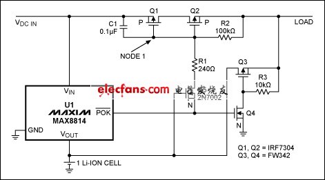
Figure 1. This circuit connects the load either to the battery voltage or to VDC IN, depending on which voltage is higher.
The Figure 1 circuit manages load switching without intervention from a microcontroller or system software. When operating on batteries and with VDC IN disconnected, the POK (Power OK) output for the MAX8814 is high. This condition connects load and battery by turning on Q4 and Q3. Node 1 is biased to the battery voltage through R2, which maintains Q1 and Q2 OFF. When VDC IN connects to a DC source, Q1 and Q2 are held OFF because C1 raises node 1 to VBATT + VDC.
High voltage at the gates of Q1 and Q2 is generated instantly when VDC IN is applied. To prevent damage at the POK input, Q5 is configured as a source follower (voltage buffer). With the gate biased to the battery voltage, POK sees no voltage higher than the battery voltage. When POK goes low, current flows through Q5 and pulls down the gates of Q1 and Q2, turning them ON. VDC IN services the load, and the charger IC (U1) charges the battery. C1 and R1 provide a short delay that allows Q3 time to turn off, preventing unregulated current from flowing to the battery.
When VDC IN is removed, POK becomes a high-impedance node, and battery current flows through the body diode of Q3. The load voltage is VBATT - VDIODE. Because Q5's gate is biased at the battery voltage, Q5 conducts until POK reaches a voltage level sufficient to to service the load by turning on Q4 and Q3. Figure 2 shows the response of the Figure 1 circuit (with battery installed), while VDC IN is applied and removed.
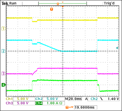
Figure 2. These waveforms illustrate behaviour of the Figure 1 circuit as the load is switched from DC power to battery and back to DC power. (CH1 is voltage across the load, CH2 is the DC supply voltage, CH3 is the active-low POK output, and CH4 is the battery current.)
A modified circuit (Figure 3) is suitable for battery-charging ICs such as the MAX1507, which does not provide a POK output. The comparator (U3) provides a POK output by comparing VDC IN to the battery voltage. Like Figure 2, Figure 4 shows voltage at the load when VDC IN is applied and removed, for the Figure 3 circuit with battery installed.
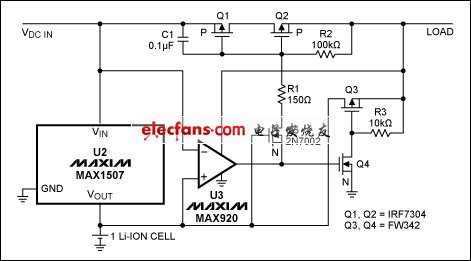
Figure 3. For battery-charger ICs without a POK output, this circuit performs the same function as that of Figure 1.
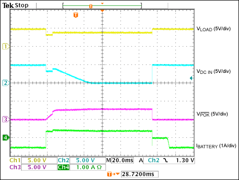
Figure 4. These waveforms illustrate behaviour of the Figure 3 circuit as the load is switched from DC power to battery and back to DC power. (CH1 is voltage across the load, CH2 is the DC supply voltage, CH3 is the active-low POK output, and CH4 is the battery current.)
-
How to Design Battery Charger2009-10-29 538
-
请问Battery supply和charger supply分别是什么,都接什么样的电源?2019-06-04 0
-
multisim 的 非理想电池 NON_IDEAL_BATTERY 为什么不起作用?2021-11-21 0
-
AVR450 pdf datasheet (Battery2008-09-03 566
-
Load-Disconnect Switch Consume2009-04-30 343
-
Battery charger and method of2009-11-28 502
-
UCC3956,pdf(Switch Mode Lithiu2010-11-09 540
-
One-Hour Battery Charger Has S2009-04-30 1190
-
Battery Backup with Delay(具有时滞2009-07-29 1674
-
Wind-Powered Battery Charger (2009-12-09 1362
-
汽车电池充电器电路 (Car Battery Charger2009-12-29 2093
-
MAX16171: Ideal Diode Controller with Reverse-Current Protection Data Sheet MAX16171: Ideal Diode Controller with Reverse-Current Protection2023-10-17 14
全部0条评论

快来发表一下你的评论吧 !
