

如何在FPGA中进行简单和复杂的数学运算?
可编程逻辑
描述
FPGA 非常适合进行数学运算,但是需要一点技巧,所以我们今天就看看如何在 FPGA 中进行简单和复杂的数学运算。
介绍
由于FPGA可以对算法进行并行化,所以FPGA 非常适合在可编程逻辑中实现数学运算。我们可以在 FPGA 中使用数学来实现信号处理、仪器仪表、图像处理和控制算法等一系列应用。这意味着 FPGA 可用于从自动驾驶汽车图像处理到雷达和飞机飞行控制系统的一系列应用。
因为 FPGA 寄存器丰富并且包含专用乘法器累加器 (DSP48) 等功能,所以在 FPGA 中实现数学运算需要一些技巧。
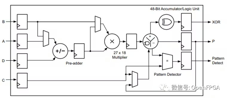
这使它们成为实现定点数学运算的理想选择,但是这与我们倾向于使用的浮点运算不同,因此在进行浮点运算时候我们需要一点技巧。
定点数学运算
定点数的小数点位于向量中的固定位置。小数点左边是整数元素,小数点右边是小数元素。这意味着我们可能需要使用多个寄存器来准确量化数字。幸运的是 FPGA 中的寄存器通常很多。

相比之下,浮点数可以存储比固定寄存器宽度(例如,32 位)宽得多的范围。寄存器的格式分为符号、指数和尾数,小数点可以浮动,因此直接使用 32 位寄存器时,其能表达的值远远超过 2^32-1。
然而,在可编程逻辑中实现定点数学运算有几个优点,而且实现起来要简单得多。由于定点解决方案使用的资源显着减少,因此可以更轻松地进行布线,从而提高性能,因此在逻辑中进行定点数学运算时可以实现更快的解决方案。
需要注意的一点是,在处理定点数学运算时会使用一些规则和术语。第一个也是最重要的问题之一是工程师如何描述向量中小数点的位置。最常用的格式之一是 Q 格式(长格式的量化格式)。Q 格式表示为 Qx,其中 x 是数字中小数位数。例如,Q8 表示小数点位于第 8 和第 9 个寄存器之间。
我们如何确定必要的小数元素的数量取决于所需的精度。例如,如果我们想使用 Q 格式存储数字 1.4530986319x10^-4,我们需要确定所需的小数位数。
如果我们想使用 16 个小数位,我们将数字乘以 63356 (2^16),结果将是 9.523023。这个值可以很容易地存储在寄存器中;然而,它的精度不是很好,因为我们不能存储小数元素,所以因为9.523023≈9, 9/65536 = 1.37329101563x10^-4。这会导致准确性下降,从而可能影响最终结果。
我们可以使用 28 个小数位,而不是使用 16 个小数位,结果就是 39006(1.4530986319x10^-4 x 2^28) 的值存储在小数寄存器中。这给出了更准确的量化结果。
了解了量化的基础知识后,下一步就是了解有关数学运算小数点对齐的规则。如果我们执行运算操作但是小数点没有对齐,我们就不会得到正确的结果。
加法——小数点必须对齐
减法——小数点必须对齐
除法——小数点必须对齐
乘法——小数点不需要对齐
我们还需要考虑操作对结果向量的影响。不考虑结果的大小可能会导致溢出。下表显示了结果大小调整的规则。
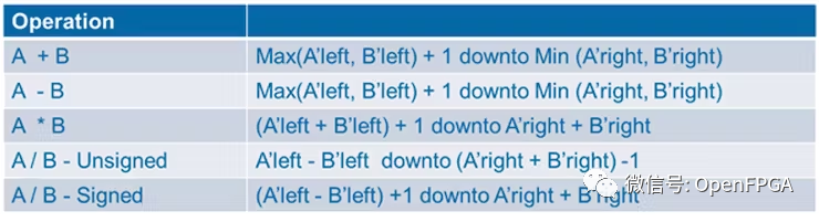
假设我们有两个向量(一个 16 位,另一个 8 位),在进行运算的时候将出现以下情况:
C(16 downto 0)= A(15 downto 0)+ B(7 downto 0)
C(16 downto 0)= A(15 downto 0)- B(7 downto 0)
C(22 downto 0)= A(15 downto 0)* B(7 downto 0)
C(8 downto -1)= A(15 downto 0)/ B(7 downto 0)
做除法时的 -1 ,反映了小数元素的寄存器大小的增加。根据所使用的类型,如果使用 VHDL 定点包,这可能是 8 到 -1,如果使用 Q1 时可能是 9 到 0。
关于除法的最后一点说明它可能会占用大量资源,因此通常最好尽可能使用移位实现除法运算。
简单算法
现在我们了解了定点数学的规则,让我们来看看我们如何能够实现一个简单的算法。在这种情况下,我们将实现一个简单的滑动平均(exponential moving average)函数。
要开始使用此应用程序,我们需要先打开一个新的 Vivado 项目并添加两个文件。第一个文件是源文件,第二个文件是测试文件。
library IEEE;
use IEEE.STD_LOGIC_1164.ALL;

--library ieee_proposed;
use ieee.fixed_pkg.all;

entity math_example is port(
 clk : in std_logic;
 rst : in std_logic;

 ip_val : in std_logic;
 ip : in std_logic_vector(7 downto 0);

 op_val : out std_logic;
 op : out std_logic_vector(7 downto 0));

end math_example;

architecture Behavioral of math_example is

constant divider : ufixed(-1 downto -16):= to_ufixed( 0.1, -1,-16 ) ;

signal accumulator : ufixed(11 downto 0) := (others => '0');
signal average : ufixed(11 downto -16 ) := (others => '0');

begin

acumm : process(rst,clk)
begin

 if rising_edge(clk) then
    if rst = '1' then
        accumulator <= (others => '0');
        average <= (others => '0');
    elsif ip_val = '1' then
        accumulator <= resize (arg => (accumulator + to_ufixed(ip,7,0)-average(11 downto 0)), size_res => accumulator);
        average <= accumulator * divider;
    end if;
 end if;
end process;

op <= to_slv(average(7 downto 0));

end Behavioral;
测试文件如下所示:
library IEEE;
use IEEE.STD_LOGIC_1164.ALL;
use ieee.numeric_std.all;

entity tb_math is
--  Port ( );
end tb_math;

architecture Behavioral of tb_math is

component math_example is port(
 clk : in std_logic;
 rst : in std_logic;

 ip_val : in std_logic;
 ip : in std_logic_vector(7 downto 0);

 op_val : out std_logic;
 op : out std_logic_vector(7 downto 0));

end component math_example;

type input is array(0 to 59) of integer range 0 to 255;

signal stim_array : input := (70,71,69,67,65,68,69,66,65,72,70,69,67,65,70,64,69,65,68,64,69,70,72,68,65,72,69,67,67,68,70,71,69,67,65,68,69,66,65,72,70,69,67,65,70,64,69,65,68,64,69,70,72,68,65,72,69,67,67,68);

constant clk_period : time := 100 ns;
signal clk : std_logic := '0';
signal rst :  std_logic:='0';
signal ip_val :  std_logic :='0';
signal ip :  std_logic_vector(7 downto 0):=(others=>'0');
signal op_val :  std_logic :='0';
signal op : std_logic_vector(7 downto 0):=(others=>'0');

begin

clk_gen : clk <= not clk after (clk_period/2);

uut: math_example port map(clk, rst, ip_val, ip, op_val, op);

stim : process
begin
 rst <= '1' ;
 wait for 1 us;
 rst <= '0';
 wait for clk_period;
 wait until rising_edge(clk);
 for i in 0 to 59 loop
  wait until rising_edge(clk);
  ip_val <= '1';
  ip <= std_logic_vector(to_unsigned(stim_array(i),8));
  wait until rising_edge(clk);
  ip_val <= '0';
 end loop;
 wait for 1 us;
 report "simulation complete" severity failure;
end process;


end Behavioral;
这些文件利用了 VHDL 2008 包文件。
让我们一步一步地看一下这些文件以及它们在做什么:
Clock - 模块的同步时钟
Reset - 将模块复位为已知状态
Input Valid (op_val) - 这表示新的输入值可用于计算
ip = 8 bit (7 downto 0) - 输入平均值
Output Valid (in_val) - 这表示计算后的值可用
op = 8 bit (7 downto 0) - 输出平均值
entity math_example is port(
 clk : in std_logic;
 rst : in std_logic;

 ip_val : in std_logic;
 ip : in std_logic_vector(7 downto 0);

 op_val : out std_logic;
 op : out std_logic_vector(7 downto 0));

end math_example;
我们架构的第一部分是除法器,它是一个常数。它被定义为无符号定点类型 (ufixed),因为我们使用的是无符号数。这是完全小数,没有整数位,所以我们将它定义为从 -1 到 -16。
constant divider : ufixed(-1 downto -16):= to_ufixed( 0.1, -1,-16 ) ;
精度可以通过以下方式确定:
0.1 x 2^16 = 6553.6
6553/2^16 = 0.999 = 99.9% 准确度
To_ufixed (0.1, -1, -16)
0.1 -我们要转换的值
-1 -数组的上限
-16 -数组的下界
信号累加器 - 存储我们的值
初始化为0进行仿真
最多可以累加 10 个 8 位值。
如果所有 10 个 8 位数字都达到其最大计数 (max = 255) 并将它们加在一起,我们将需要一个 12 位数字,因此我们将 ufixed 定义为 (11 downto 0)。
我们只存储整数位,没有小数位。
signal accumulator : ufixed(11 downto 0) := (others => '0');
信号平均值-输出值
初始化为0进行仿真
12 位数字(整数)乘以 0.1(我们的分频器数字),结果为 -16。这给了我们 11 downto -16 的范围。
signal average : ufixed(11 downto -16 ) := (others => '0');
让我们继续看代码——有一个同步复位的进程。在使用 AMD FPGA时,我们应该使用同步复位。
如果对模块进行复位,那么将会对所有内容设置为零。
if rising_edge(clk) then
    if rst = '1' then
        accumulator <= (others => '0');
        average <= (others => '0');
如果复位信号为“0”,则在时钟的上升沿并且输入有效 (ip_val) = 1,进行以下操作:
将获取输入值(作为标准逻辑向量出现),将其添加到当前累加器值
To_ufixed (ip, 7, 0) - VHDL 会将值从标准逻辑向量转换为无符号定点
然后,因为它是滑动平均值,将从累加器中减去之前的平均值
elsif ip_val = '1' then
        accumulator <= resize (arg => (accumulator + to_ufixed(ip,7,0)-average(11 downto 0)), size_res => accumulator);
完成累加后,我们将累加器的值乘以"除法器"(乘法器实现的除法器)
average <= accumulator * divider;
最后我们输出结果缩放平均值
op <= to_slv(average(7 downto 0));
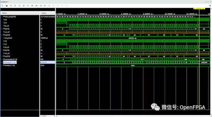
仿真结果如下:
上面就简单介绍了一个简单的运算系统,该系统使用加法、减法和乘法代替除法。
然而,我们可能会面临需要在 FPGA 中实现的更复杂的数学运算。
复杂算法
更复杂的算法可能具有挑战性,例如用于将 PRT 电阻转换为温度的 Callendar-Van Dusen 方程:
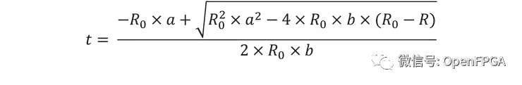
上面的公式,简单的运算我们知道怎么实现,但是平方根是一个新的运算,我们可以使用 CORDIC 算法实现平方根。
上面说的很简单,但是实施起来却很复杂,并且验证过程中要捕获所有极端情况会很耗时。
如果我们在感兴趣的温度范围内绘制方程,我们可以采用更好的方法-使用多项式近似方式。
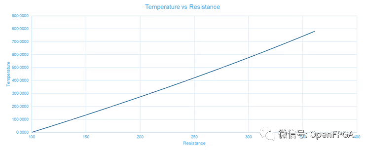
我们可以从此图中提取趋势线:
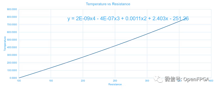
在 FPGA 中实现这个多项式方程比实现上面所示的复杂方程要容易得多。
我们需要做的第一件事是量化参数,为此,我们需要使用 Excel (MatLab也行)进行相关的数据处理。
通过上面的表格计算出量化参数,接下来就可以使用HDL实现算法。这次我们将使用二进制补码的符号数字进行运算。
完整的实现如下所示
library IEEE;
use IEEE.STD_LOGIC_1164.ALL;

use ieee.fixed_pkg.all;

entity complex_example is port(

clk : in std_logic;

ip_val : in std_logic;
ip     : in std_logic_vector(7 downto 0);
op_val : out std_logic;
op     : out std_logic_vector(8 downto 0));

end complex_example;

architecture Behavioral of complex_example is

type fsm is (idle, powers, sum, result);

signal current_state : fsm := idle;
signal power_a : sfixed(35 downto 0):=(others=>'0');
signal power_b : sfixed(26 downto 0):=(others=>'0');
signal power_c : sfixed(17 downto 0):=(others=>'0');

signal calc  : sfixed(49 downto -32) :=(others=>'0');
signal store : sfixed(8 downto 0) := (others =>'0');

constant a : sfixed(9 downto -32):= to_sfixed( 2.00E-09, 9,-32 );
constant b : sfixed(9 downto -32):= to_sfixed( 4.00E-07, 9,-32 );
constant c : sfixed(9 downto -32):= to_sfixed( 0.0011, 9,-32 );
constant d : sfixed(9 downto -32):= to_sfixed( 2.403, 9,-32 );
constant e : sfixed(9 downto -32):= to_sfixed( 251.26, 9,-32 );

begin

cvd : process(clk)
begin
 if rising_edge(clk) then
  op_val <='0';
  case current_state is
   when idle =>
    if ip_val = '1' then
     store <= to_sfixed('0'&ip,store);
     current_state <= powers;
    end if;
   when powers =>
    power_a <= store * store * store * store;
    power_b <= store * store * store;
    power_c <= store * store;
    current_state <= sum;
   when sum =>
    calc <= (power_a*a) - (power_b * b) + (power_c * c) + (store * d) - e;
    current_state <= result;
   when result =>
    current_state <= idle;
    op <= to_slv(calc(8 downto 0));
    op_val <='1';
   end case;
  end if;
end process;

end Behavioral;
加下来我们简单介绍下代码:
时钟 (clk) - 驱动模块的主时钟
Input Valid (ip_val) 和 Input (ip) - 表示我们在 8 位输入上有有效数据(7 downto 0)
Output Valid (op_val) 和 Output (op) - 一旦我们运行了我们的算法,我们输出一个 9 位数(8 downto 0)
entity complex_example is port(

clk : in std_logic;

ip_val : in std_logic;
ip     : in std_logic_vector(7 downto 0);
op_val : out std_logic;
op     : out std_logic_vector(8 downto 0));

end complex_example;
接下来我们做的是为状态机定义状态,状态机中有 4 个状态:
Idle- 从第一个状态开始等待输入有效
Powers- 计算
Sum - 将所有的算子相加
Result- 将结果传递给下游模块
type fsm is (idle, powers, sum, result);
在类型声明之后是我们在设计中使用的信号
计算出的信号 a-c 当它们在算法中被提升到各自的幂时。
用于存储每个结果的位数取决于输入的大小和它们的幂次。首先要做的是将 8 位无符号数转换为 9 位有符号数。然后对于 power_a,生成的向量大小是四次九位向量乘法,这意味着一个 36 位向量。对于 power_b,这是三个九位向量乘法等等。
signal power_a : sfixed(35 downto 0):=(others=>'0');
signal power_b : sfixed(26 downto 0):=(others=>'0');
signal power_c : sfixed(17 downto 0):=(others=>'0');
计算结果-输出值的计算结果位宽 -49 downto -32
Signal Store - 转换为有符号数时我们存储输入的转换
我们的输入被转换成什么。
这是一个 9 位存储,代表 8 位加上一个符号位来组成 9 位
实际输入永远不会是负数,因为输入代表一个大约在 70 欧姆到几百欧姆之间的电阻值
signal calc  : sfixed(49 downto -32) :=(others=>'0');
signal store : sfixed(8 downto 0) := (others =>'0');
常数 ae - 先前在 excel 中使用 Callendar-Van Dusen 方程计算的系数
to_sfixed 中的第一个值是电子表格中的值
第二个值是我们存储值的整数位数。在本例中它是 9 位,因为常量需要达到 251.26 的值
第三个值是我们将使用的小数位数,它是 -32,由 2.00E-09 的最低常量值决定。定义小数位数是我们有效计算量化的地方
constant a : sfixed(9 downto -32):= to_sfixed( 2.00E-09, 9,-32 );
constant b : sfixed(9 downto -32):= to_sfixed( 4.00E-07, 9,-32 );
constant c : sfixed(9 downto -32):= to_sfixed( 0.0011, 9,-32 );
constant d : sfixed(9 downto -32):= to_sfixed( 2.403, 9,-32 );
constant e : sfixed(9 downto -32):= to_sfixed( 251.26, 9,-32 );
在时钟的上升沿,该过程将被执行。op_val 是默认赋值,除非在流程的其他地方将其设置为“1”,否则它将始终为“0”输出。在进程中,信号被分配最后一个分配给它们的值,默认分配使代码更具可读性。
Idle状态 -如果一个值进来(ip_val) = 1,那么
我们将值加载到存储寄存器并将符号位设置为 0 (指示正数)
然后状态机进入Power状态。
if ip_val = '1' then
     store <= to_sfixed('0'&ip,store);
     current_state <= powers;
end if;
Power 状态- 在Power状态下,我们计算三个幂运算,然后进入求和状态。
Power a - 将存储的值乘以自身 4 次。Power b - 将存储的值乘以自身 3 倍Power c - 将存储的值乘以自身 2 倍
when powers =>
    power_a <= store * store * store * store;
    power_b <= store * store * store;
    power_c <= store * store;
    current_state <= sum;
Sum状态——这是我们将所有值输入 excel 图表的多项式近似值并进行加法和减法以获得最终输出值的地方。
请注意,无论我们的数字有多大,上面定义的常量都将小数点对齐到 -32 位,这对于计算总和很重要。
 calc <= (power_a*a) - (power_b * b) + (power_c * c) + (store * d) - e;
 current_state <= result;
Results状态- 此处我们采用最终值(并将其作为标准逻辑向量放入输出中。断言 Op_val 表示存在新的输出值)。
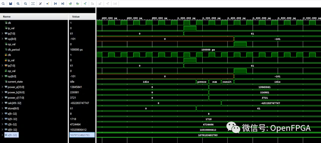
下面的仿真文件用来仿真这次的算法核心。
library IEEE;
use IEEE.STD_LOGIC_1164.ALL;

use IEEE.NUMERIC_STD.ALL;


entity tb_complex is
--  Port ( );
end tb_complex;

architecture Behavioral of tb_complex is

component complex_example is port(
clk    : in std_logic;
ip_val : in std_logic;
ip     : in std_logic_vector(7 downto 0);
op_val : out std_logic;
op     : out std_logic_vector(8 downto 0));
end component complex_example;


signal clk    :  std_logic:='0';
signal ip_val :  std_logic:='0';
signal ip     :  std_logic_vector(7 downto 0):=(others=>'0');
signal op     :  std_logic_vector(8 downto 0):=(others=>'0');
signal op_val :  std_logic:='0';
constant clk_period : time := 100 ns;

begin

clk <= not clk after (clk_period/2);

uut: complex_example port map(clk,ip_val,ip,op_val,op);

stim : process
begin
 wait for 1 us;
 wait until rising_edge(clk);
 ip_val <= '1';
 ip <= std_logic_vector(to_unsigned(61,8));
 wait until rising_edge(clk);
 ip_val <= '0';
 wait for 1 us;
 report " simulation complete" severity failure;
end process;


end Behavioral;
仿真结果如下:
总结
在这个项目中,从简单算法到复杂算法,我们逐步了解了如何使用 HDL 在 FPGA 上进行数学运算。
审核编辑:刘清
-
用labvIEW进行复杂的数学运算的时候,有怎样的思路?2012-04-25 0
-
求MATLAB偏微分数学运算编程,限定时间完成,有酬谢.2013-02-17 0
-
单片机实现算法和进行复杂的运算2022-01-07 0
-
鼎阳示波器功能之数学运算2022-05-10 0
-
如何在GCC中为具有FPU的Cortex M4启用硬件浮点数学运算呢?2022-08-26 0
-
基本数学运算库VHDL代码2008-05-20 828
-
基本数学运算库 -包括各种用VHDL语言描述的基本数学运算单2009-06-14 595
-
GE FANUC PLC的数学运算功能2009-11-14 550
-
CCS及DSP基本数学运算实验2010-04-06 591
-
基于GPU的数学形态学运算并行加速研究2011-10-25 1070
-
简单的数学运算计算数学函数的方法CORDIC的详细资料概述2018-05-31 818
-
关于Tcl中的数学运算2018-09-04 8923
-
数学运算在FPGA中的实现方式2022-10-31 2540
-
Python中常见的数学运算方法2023-04-21 4886
-
C语言中关于数学运算的相关知识2023-11-08 312
全部0条评论

快来发表一下你的评论吧 !
