

Microchip PIC系列8位单片机入门教程(6)ADC
控制/MCU
描述
第一节 知识点
1.ADC
(1)10 位模数转换器(A/D)模块:28 引脚器件的模数(Analog-to-DigitalA/D)转换器具有10 路输入,而40/44 引脚器件的模数转换器则具有13 路输入。A/D 模块能将一个模拟输入信号转换成相应的10 位数字信号。
(2)此模块有五个寄存器:
• A/D 转换结果高位寄存器(ADRESH)
• A/D 转换结果低位寄存器(ADRESL)
• A/D 转换控制寄存器0 (ADCON0):A/D 模块的工作方式由ADCON0寄存器控制。
• A/D 转换控制寄存器1 (ADCON1):端口引脚的功能由ADCON1 寄存器配置。
• A/D 转换控制寄存器2 (ADCON2):由ADCON2 寄存器配置A/D 时钟源,编程采集时间和对齐方式。
(3)执行A/D 转换时应该遵循以下步骤:
- 配置A/D 模块:
• 配置模拟引脚、参考电压和数字I/O (通过ADCON1 寄存器)
• 选择A/D 输入通道(通过ADCON0 寄存器)
• 选择A/D 采集时间(通过ADCON2 寄存器)
• 选择A/D 转换时钟(通过ADCON2 寄存器)
• 使能A/D 模块(通过ADCON0 寄存器) - 需要时,配置A/D 中断:
• 清零ADIF 位
• 将ADIE 位置1
• 将GIE 位置1 - 如果需要,等待所需的采集时间。
- 启动转换:
• 将GO/DONE 位置1 (ADCON0 寄存器) - 等待A/D 转换完成,通过以下两种方法之一判断转换是否完成:
• 查询GO/DONE 位是否被清零或 等待A/D 中断 - 读取A/D 结果寄存器(ADRESH:ADRESL),需要时将ADIF 位清零。
- 如需再次进行A/D 转换,返回步骤1 或步骤2。将每位的A/D 转换时间定义为TAD,在下一次采集开始前至少需要等待2 个TAD。
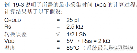
(4)A/D 采集要求
为了使A/D 转换器达到规定精度,必须使充电保持电容(CHOLD)充满至输入通道的电平。图19-3 给出了模拟输入的电路模型。电源阻抗(RS)和内部采样开关阻抗(RSS)直接影响电容CHOLD 充电的时间。采样开关(RSS)阻抗值随器件电压(VDD)不同而改变。电源阻抗将影响模拟输入的偏移电压(由于引脚泄漏电流的原因)。模拟信号源的最大阻抗推荐值为2.5 kΩ。在选择(改变)了模拟输入通道之后,必须对通道进行采样才能启动转换,采样时间必须大于最小采集时间。
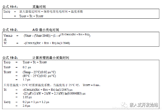
(5) 采样时间计算:
1.ADC的原理框图: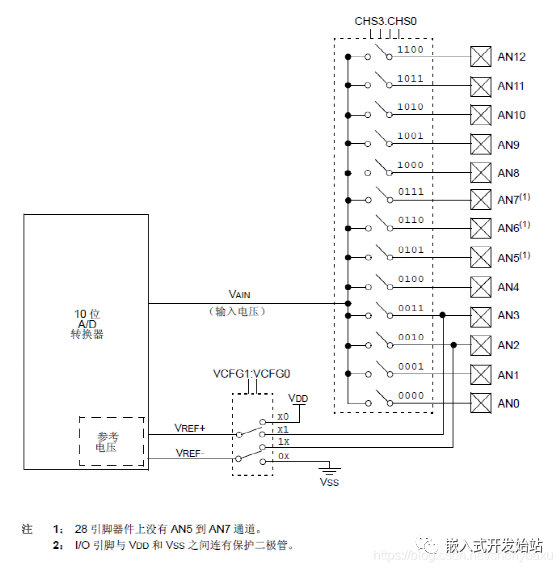
2.与ADC相关的寄存器: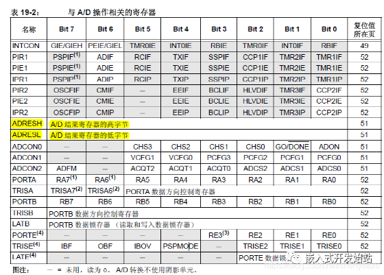
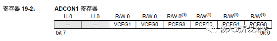
我们设置VCFG1=0,采用BSS作为参考电压VREF-;
设置VCFG0=0,采用VDD作为VREF+的参考电压。
配置PCFG3:PCFG0 进行采集模拟量的端口配置。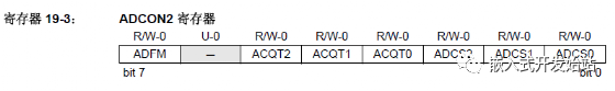
配置ADFM,ADC转化结构的格式是左对齐还是右对齐,这是因为ADC转化结果是10位的需要两个8位寄存器存储。
ACQT2:ACQT0:A/D 采集时间选择位;
ADCS2:ADCS0:A/D 转换时钟选择位。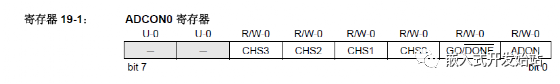
3.比如我们在实际中要采集电压,典型的电路图如下: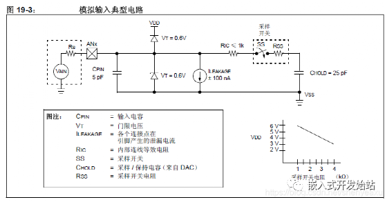
02第二节 代码设计
1.我们新建两个文件:
(1) adc_sample.h
/* Microchip Technology Inc. and its subsidiaries.  You may use this software
* and any derivatives exclusively with Microchip products.
* File:   adc_sample.h
* Author: Greg
* Comments:
* Revision history:  2018-06-21
*/


// This is a guard condition so that contents of this file are not included
// more than once.
#ifndef _ADC_SAMPLE_H_
#define           _ADC_SAMPLE_H_


#include // include processor files - each processor file is guarded.


#define Channel_0_ON 0b0000
#define Channel_1_ON 0b0001
#define Channel_2_ON 0b0010
#define Channel_3_ON 0b0011
#define Channel_4_ON 0b0100
#define Channel_5_ON 0b0101
#define Channel_6_ON 0b0110
#define Channel_7_ON 0b0111
#define ADC_Channel_select ADCON0bits.CHS
#define ADC_ENABLE ADCON0bits.ADON=1
#define ADC_DISABLE ADCON0bits.ADON=0
#define ADC_STATUS ADCON0bits.GODONE
#define ADC_START ADCON0bits.GO=1
#define ADC_PORT_DIR TRISA


void ADC_Channel_config(void);
double ADC_Converter_Ddecimal(unsigned int ADC_data);
double ADC_Process_show(unsigned char Channel_selected );
double ADC_Process_Select_work(unsigned char Channel_selected);
#endif           /* XC_HEADER_TEMPLATE_H */
(2)adc_sample.c
#include
#include "adc_sample.h"
static unsigned int  ADC_Data[8]=0;
void ADC_Channel_config(void)
{
    ADC_PORT_DIR=0xFF;
    ADCON1bits.PCFG=0b0111; //select An0-An7 Channel to A_D converter
    ADCON1bits.VCFG=0b00;   //voltage reference for Vss,Vdd.
    ADCON2bits.ADFM=1;  // reslut right justed
    ADCON2bits.ACQT=0b001;
    ADCON2bits.ADCS=0b000;
}
/*
this fucntion is to converter result of ADC to decimal result.
*/
double ADC_Converter_Ddecimal(unsigned int ADC_data)
{   double temp;
    temp=(double) ADC_data*5.0;
     return temp/1023.0;
}


/*
* This is first way to get ADC sample Result.
*/
double ADC_Process_show(unsigned char Channel_selected)
{
    double ADC_temp0=0;
    switch (Channel_selected){
            case 0:
                ADC_Channel_select=Channel_0_ON;
                break;
            case 1:
                ADC_Channel_select=Channel_1_ON;
                break;
            case 2:
                ADC_Channel_select=Channel_2_ON;
                break;
            case 3:
                ADC_Channel_select=Channel_3_ON;
                break;
            case 4:
                ADC_Channel_select=Channel_4_ON;
                break;
            case 5:
                ADC_Channel_select=Channel_5_ON;
                break;
            case 6:
                ADC_Channel_select=Channel_6_ON;
                break;
            case 7:
                ADC_Channel_select=Channel_7_ON;
                break;}
    ADC_ENABLE;
    ADC_START;
    while(ADC_STATUS);
//    ADC_Data[0]=0x00FF&ADRESL;
//    ADC_Data[0]|=ADRESH< < 8;< span="" >
    ADC_Data[0]=ADRES;
    ADC_temp0=ADC_Converter_Ddecimal(ADC_Data[Channel_selected]);
    return ADC_temp0;
}


/*
* This is second way to get ADC sample Result.
*/


double ADC_Process_Select_work(unsigned char Channel_selected)
{   double ADC_temp0=0;
    ADC_Channel_select=Channel_selected;
    ADC_ENABLE;
    ADC_START;
    while(ADC_STATUS);
//    ADC_Data[0]=0x00FF&ADRESL;
//    ADC_Data[0]|=ADRESH< < 8;< span="" >
    ADC_Data[0]=ADRES;
    ADC_temp0=ADC_Converter_Ddecimal(ADC_Data[0]);
    return ADC_temp0;
}
(3)main.C
// PIC18F4520 Configuration Bit Settings


// 'C' source line config statements
// Author:Greg
// Title:ADC 采样
// CONFIG1H
#pragma config OSC = HS         // Oscillator Selection bits (HS oscillator)
#pragma config FCMEN = OFF      // Fail-Safe Clock Monitor Enable bit (Fail-Safe Clock Monitor disabled)
#pragma config IESO = OFF       // Internal/External Oscillator Switchover bit (Oscillator Switchover mode disabled)


// CONFIG2L
#pragma config PWRT = OFF       // Power-up Timer Enable bit (PWRT disabled)
#pragma config BOREN = SBORDIS  // Brown-out Reset Enable bits (Brown-out Reset enabled in hardware only (SBOREN is disabled))
#pragma config BORV = 3         // Brown Out Reset Voltage bits (Minimum setting)


// CONFIG2H
#pragma config WDT = OFF        // Watchdog Timer Enable bit (WDT disabled (control is placed on the SWDTEN bit))
#pragma config WDTPS = 32768    // Watchdog Timer Postscale Select bits (1:32768)


// CONFIG3H
#pragma config CCP2MX = PORTC   // CCP2 MUX bit (CCP2 input/output is multiplexed with RC1)
#pragma config PBADEN = ON      // PORTB A/D Enable bit (PORTB< 4:0 >pins are configured as analog input channels on Reset)
#pragma config LPT1OSC = OFF    // Low-Power Timer1 Oscillator Enable bit (Timer1 configured for higher power operation)
#pragma config MCLRE = OFF      // MCLR Pin Enable bit (RE3 input pin enabled; MCLR disabled)


// CONFIG4L
#pragma config STVREN = OFF     // Stack Full/Underflow Reset Enable bit (Stack full/underflow will not cause Reset)
#pragma config LVP = OFF        // Single-Supply ICSP Enable bit (Single-Supply ICSP disabled)
#pragma config XINST = OFF      // Extended Instruction Set Enable bit (Instruction set extension and Indexed Addressing mode disabled (Legacy mode))


// CONFIG5L
#pragma config CP0 = OFF        // Code Protection bit (Block 0 (000800-001FFFh) not code-protected)
#pragma config CP1 = OFF        // Code Protection bit (Block 1 (002000-003FFFh) not code-protected)
#pragma config CP2 = OFF        // Code Protection bit (Block 2 (004000-005FFFh) not code-protected)
#pragma config CP3 = OFF        // Code Protection bit (Block 3 (006000-007FFFh) not code-protected)


// CONFIG5H
#pragma config CPB = OFF        // Boot Block Code Protection bit (Boot block (000000-0007FFh) not code-protected)
#pragma config CPD = OFF        // Data EEPROM Code Protection bit (Data EEPROM not code-protected)


// CONFIG6L
#pragma config WRT0 = OFF       // Write Protection bit (Block 0 (000800-001FFFh) not write-protected)
#pragma config WRT1 = OFF       // Write Protection bit (Block 1 (002000-003FFFh) not write-protected)
#pragma config WRT2 = OFF       // Write Protection bit (Block 2 (004000-005FFFh) not write-protected)
#pragma config WRT3 = OFF       // Write Protection bit (Block 3 (006000-007FFFh) not write-protected)


// CONFIG6H
#pragma config WRTC = OFF       // Configuration Register Write Protection bit (Configuration registers (300000-3000FFh) not write-protected)
#pragma config WRTB = OFF       // Boot Block Write Protection bit (Boot block (000000-0007FFh) not write-protected)
#pragma config WRTD = OFF       // Data EEPROM Write Protection bit (Data EEPROM not write-protected)


// CONFIG7L
#pragma config EBTR0 = OFF      // Table Read Protection bit (Block 0 (000800-001FFFh) not protected from table reads executed in other blocks)
#pragma config EBTR1 = OFF      // Table Read Protection bit (Block 1 (002000-003FFFh) not protected from table reads executed in other blocks)
#pragma config EBTR2 = OFF      // Table Read Protection bit (Block 2 (004000-005FFFh) not protected from table reads executed in other blocks)
#pragma config EBTR3 = OFF      // Table Read Protection bit (Block 3 (006000-007FFFh) not protected from table reads executed in other blocks)


// CONFIG7H
#pragma config EBTRB = OFF      // Boot Block Table Read Protection bit (Boot block (000000-0007FFh) not protected from table reads executed in other blocks)


// #pragma config statements should precede project file includes.
// Use project enums instead of #define for ON and OFF.


#include
#include "adc_sample.h"
#include
#include "usart_dr.h"
//#include"plib/adc.h"
//#include "delays.h"
int main(void)
{
   unsigned char Channel_select=0;
    double ADC_temp0;
    ADC_Channel_config();
    usart_port_dir_init();
    usart_Config_init();
    printf("test for printf functionrtn"); // printf 函数实现成功!
    printf("ADC 采样实现rtn"); // printf 函数实现成功!
    while(1)
    {
       ADC_temp0=ADC_Process_show(Channel_select);
       printf("ADC var:%frtn",ADC_temp0);
       ADC_temp0=ADC_Process_Select_work(Channel_0_ON);
        printf("ADC var:%frtn",ADC_temp0);
    }
     return 0;
}
下载到开发板中看效果吧,代码的注释很清楚我就不解释了。
-
Microchip推出全新通用小型PIC单片机彰显最新技术成果2008-07-09 0
-
PIC单片机开发环境(教程)2011-03-04 0
-
PIC 8位单片机16F8X系列简介2011-09-30 0
-
全新低引脚数32位PIC32单片机-Cogobuy商城最新报道2012-03-15 0
-
PIC单片机与51系列单片机的区别2012-07-21 0
-
PIC8位单片机的基本组成2012-12-01 0
-
Microchip的PIC系列单片机开发板选用指南2014-08-29 0
-
【秀秀资源】STM8单片机相关资料2017-03-21 0
-
PIC系列单片机的主要应用领域2021-11-24 0
-
单片机入门教程2006-03-21 2491
-
PIC单片机图解入门教程2011-05-26 1888
-
单片机入门教程[1]2016-06-17 604
-
Microchip图形库与PIC单片机2021-11-16 747
-
Microchip PIC系列8位单片机入门教程(2):点亮LED灯2023-07-14 1584
全部0条评论

快来发表一下你的评论吧 !
