

浅谈Via stub在DDR4并行链路上的表现
存储技术
描述
编者注:这是DesignCon2020年的最佳论文之一。做高速链路的小伙伴都知道,Stub总是会带来各种影响,或者导致阻抗突变,或者导致插入损耗曲线上存在谐振,等等。本文介绍了Via stub在DDR4并行链路上的表现。下面是论文的全文。
As PCBs continue to become more complex with higher densities, this drives an increase in the number of layers in a PCB stack-up used to ensure all signals in the design are routed effectively. Thick PCB vias with long stubs create unwanted resonances in the channel, whereas vias with short or no stubs do not. If these resonances occur near the Nyquist frequency of the bit rate, they will devastate the eye opening at the receiver [3]. In this case for DDR4-3200, the Nyquist frequency is the clock frequency at 1.6 GHz.
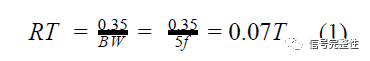
A rule of thumb that some of us might be familiar with is that the interconnect bandwidth (BW) should be five times the Nyquist frequency of the bit rate to preserve integrity of the rise time down to 7 percent of the clock period [4]. In other words, the resonant frequency of the DDR4 channel should be five times greater than the DDR4 clock frequency to preserve the signal. This will be important later after results are presented. This rule of thumb is depicted by EQ (1).
Where:
RT : 10-90 rise time, in nsec
BW : bandwidth (BW) product to the 5th harmonic of the fundamental frequency
f : Nyquist or clock frequency
T : Nyquist frequency period, equivalent to 1/f
There are various industry practices to avoid via stub issues, such as routing high-speed signals in specific layers, slowing down the channel speeds, making design tradeoffs on other portions of the channel, using high-density interconnect (HDI) manufacturing techniques like blind or buried vias, or use backdrilling to remove the via stub [11]. HDI designs are known to be very expensive, even more so in the enterprise market that uses multi-socket platforms implementing larger PCBs. HDI is also limited by a finite number of lamination cycles that a PCB can withstand, thus it is impossible to fully eliminate all via stubs on a multi-layer PCB.
Backdrilling is a widely used technology since it is an effective way of minimizing stub effects. However, backdrilling becomes challenging for denser vias, such as the via field underneath a central processing unit (CPU) and chipset package, or the stub length becomes longer on a thick board. Backdrilling cannot completely remove the stubs because of the drill depth tolerance and the manufacturing requirements on some vias, such as the ones for press-fit connectors. Generally speaking, backdrilling is not typically used for DDR applications due to the high number of signals and, therefore, the high fabrication cost.
The Problem
What is driving these challenges? Let’s consider the following design scenario with a networking product design. The PCB is 22 layers and over 100 mils in total thickness. There are multiple 10 Gbps Ethernet signals which take priority to be routed on the top and inner layers since these signals are three times faster than the DDR4-3200 signals. In addition, there are PCIe signals as well as multiple power and ground nets consuming valuable inner layers. In this scenario, the DDR4 data (DQ) signals are left to be routed on layer 3. As a result, this creates the opportunity for via stubs to greatly impact the signal integrity of these DDR signals. As iterated in a Keysight application note on DDR [5], “to improve signal performance as data transfer rates increase and signal amplitude decreases, the clock and strobe signals (DQS) are differential, which cancels out common mode noise. The other signals, specifically data (DQ), address (ADD) and control (CTL) still operate in single-ended mode, which makes them more susceptible to noise, crosstalk, and interference.” The DQ signals operate at two times the data rate as ADD and CTL signals, which make them the most critical. This raises the question, what is the maximum stub length (or discontinuity) allowed in the DDR4 channel?
Proposed Model and Setup
A DDR4 ½ byte lane was simulated using a Keysight PathWave ADS DDR bus simulator based on the test cases, and parameters defined in this section. The DDR bus simulator allows for simulation that meets the DQ receiver compliance mask at 1x10-16 BER as per JEDEC DDR4 specification. The DDR bus simulator has statistical and bit-by-bit modes. There is also a transient SPICE simulator too. All three solutions will generate the asymmetric rising and falling edges. The only simulator type that will not is the standard channel sim (known in IBIS as the Reference Flow). Standard channel sim just uses a rising edge to characterize the electrical interconnect. In SerDes links, this is enough, but for DDR, single-ended signals need a DDR bus sim approach. Transient SPICE starts to be less interesting because it won’t be able to predict eye closure down to low BERs in a practical time [6].
The DQ input receiver compliance mask defines the area that the input signal must not encroach in order for the DRAM input receiver to be expected to successfully capture a valid input signal with BER of 1x10-16; any input signal encroaching with the Rx Mask is subject to being invalid data [7]. This will be set for all BER contours during the presented analysis. The simulation results shown include only some of the crosstalk components. In addition, the simulation results do not include any DDR4 equalization enabled, which would compensate for any channel loss effects. The objective of this effort is to explore the loss in the channel.
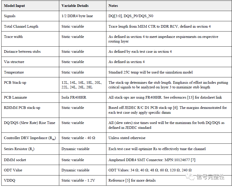
This effort will execute analysis based on the test cases defined below. Table 1 below defines the common variables used for each of the three test cases. Jitter was not injected into any test cases since that is another exercise in experimentation in itself. Therefore, the only source of jitter in the simulation is the interconnect, all the jitter is deterministic (DJ). However, it is important to point out that in a real system the results will be even worse than those presented, since random (RJ) and data-dependent jitter (DDJ) will also be included. Furthermore, no analysis will be done in simulation to explore receiver model de-emphasis and continuous-time linear equalization (CTLE). Eight PCB stack-ups were created from 14L to 28L to vary the via stub length in the DDR4 channel to determine the worst-case scenario. Those stack-up designs can be referenced in greater detail in my DesignCon 2020 paper [1]. In addition, each test case provides a depiction of the respective channel model for reference.
Table 1 - Model Variables for each Test Case
Simulation Test Cases
For this article, test case #1 has been removed. Test case #1 can be referenced in [1]. It was primarily used to establish a baseline with the simulation model with no discontinuities as part of the channel. It should be noted for this effort the entire channel length for all test cases was the same at 937 mils.
The objective of Test Case #2 is to provide a simulation model of the channel for a static total channel length, at 3200 Mbps, with only the via discontinuities included in the channel.
For all of the PCB stack-ups defined, the via structure is represented in Figure 1, and the via structure parameters are defined by Table 2. The intent was to define a via structure that would allow close to a 10:1 aspect ratio with a 10 mil via diameter that would vary from a 14L stack-up to a 28L stack-up. Therefore, the via structure parameters for this effort were selected to achieve a 10:1 aspect ratio based on a median PCB thickness of around 100 mils. Figure 2 provides a 2D depiction of the DDR4 data signal model with vias in a point-to-point scenario. Figure 3 provides the 2D depiction of the channel model between the memory controller and the DDR4 memory.
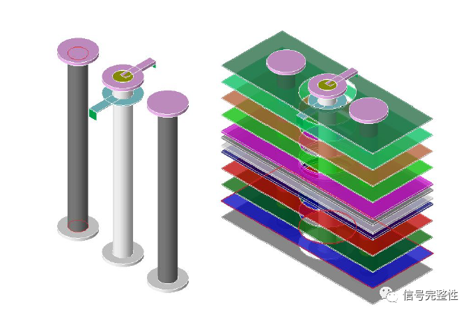
Figure 1 - Depiction of single-ended 3D Via Model Structure with feeds on L1 and L3, right image depicts via structure with plane layers enabled
Table 2 - Via Parameter Definition
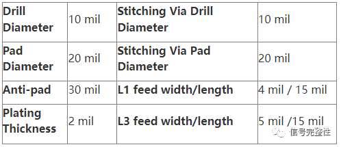
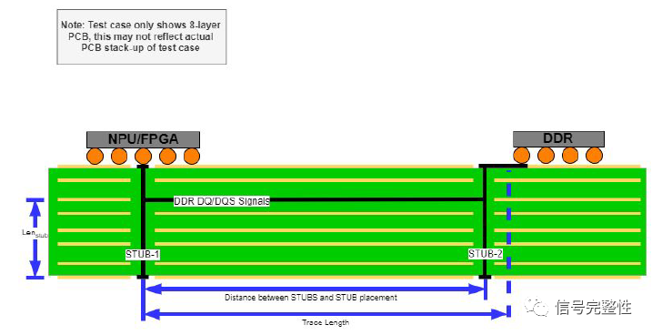
Figure 2 - Test Case #2 - 2D Model Depiction of DDR4 Data Signals Point-to-Point With Vias
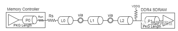
Figure 3 - Test Case #2 - DQ Channel Model of DDR4 Data Signals Point-to-Point with Vias in the Channel
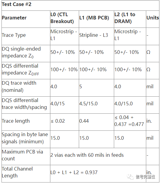
Table 3 - Test Case #2 - Impedance, Length, and Spacing Guidelines for DDR4 Signals
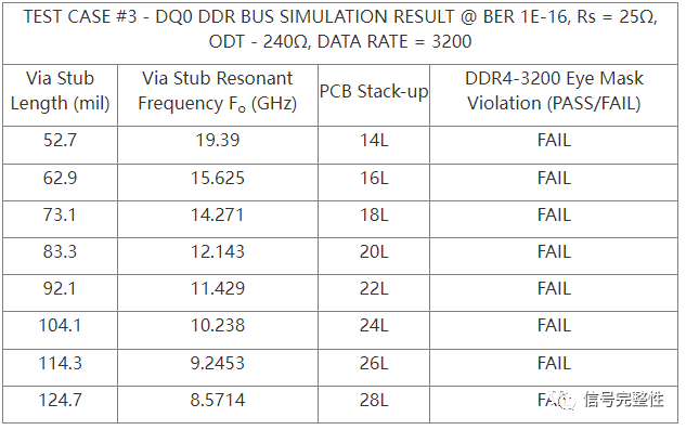
The objective of Test Case #3 is to understand if DDR4-3200 eye mask violations will occur with multiple discontinuities in the DDR4 channel including vias, the DIMM PCB, and the DIMM connector in comparison to a channel of the same length in Test Case #2 without the DIMM interconnect. Further, the limits of this test case will be explored in order to understand where eye mask failures can occur with a DIMM interconnect as part of the DDR4 channel. Figure 4 provides a 2D depiction of the DDR4 data signal model with the vias and the DDR4 DIMM. Figure 5 provides a 2D depiction of the channel model between the memory controller and the DDR4 DIMM.
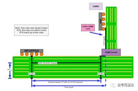
Figure 4 - Test Case #3 - 2D Model Depiction of Single DDR4 DIMM per Channel
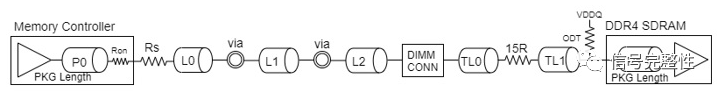
Figure 5 - Test Case #3- DQ Channel Model of Single DDR4 DIMM per Channel
Table 4 - Test Case #3 - Impedance, Length, and Spacing Guidelines for DDR4 Signals
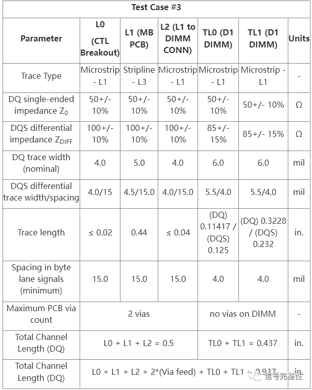
Micron has DDR4 SDRAM RDIMM - 8GB (MPN: MTA9ASF1G72PZ) that supports PC4-3200. This RDIMM is a 288-pin RDIMM (MO-309, R/C-D1 format). The R/C-D1 RDIMM is defined by JEDEC standard [8]. The RDIMM DDR4 R/C D1 fabrication table which can be referenced in that JEDEC standard [8] was used to create the ADS stack-up which can be referenced in [1] Figure A.7, which is used as part of the test case #3 simulation model. The net structure for JEDEC RDIMM DQ signals do include the 15R resistors in line with each DQ signal on the RDIMM.
Simulation and Results
For all cases, eye mask simulations are depicted as per JEDEC standard [7]; see also Table 1.
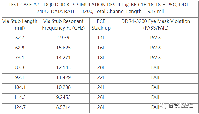
For Test Case #2, results shown below are after tuning the channel at 3200 Mbps, for the best Rs and ODT values. The results of each channel simulation can be referenced in Table 5. As shown by Figure 6, the maximum stub length to meet DDR4-3200 eye mask compliance requirements, with no equalization enabled, for a 937 mil long channel is 73.1 mils.
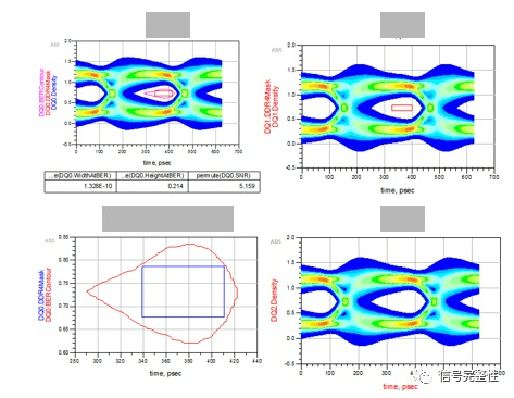
Figure 6 - Test Case #2 - DQ[0-2] - Data rate = 3200 Mbps, MB = 18L PCB (73.1 mil stubs), Rs = 25, ODT = 240, Total Channel Length = 937 mil
Table 5 - Test Case #2 Results Summary
For Test Case #3, the results shown below are after tuning the channel at 3200 Mbps, for the best Rs and ODT values. The Test Case #3 results are summarized by Table 6. Referring to Figure 7, even when the DDR4 channel uses the minimum available stub length of 52.7 mils, the DDR4 compliance eye mask requirements with data rates of 3200 MT/s still cannot be passed. So further analysis was done to route the data signals only on the top layer as a microstrips to the DIMM interconnect. In other words, no via stubs were included in the DDR4 channel.
Based on the eye diagram result shown by Figure 8, this channel with only the DIMM interconnect still does not support DDR4-3200 data rates due to the discontinuity and loss from the DIMM interconnect. Therefore, by that analysis, it was not necessary to do any further analysis on other PCB stack-ups to use shorter via stubs. Although further analysis could be done to explore alternative DIMM interconnect solutions. It is assumed since the DDR4 connector is based on a JEDEC standard these results likely will be very similar. Although, due to time constraints this will have to be done in a future effort.
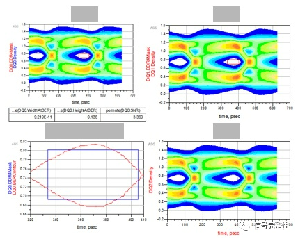
Figure 7 - Test Case #3 - DQ[0-2] - Data rate = 3200 Mbps, MB = 14L PCB (52.7 mil stubs), Rs = 25, ODT = 240, MB Channel Length = 500 mils, Total Channel Length = 937 mils
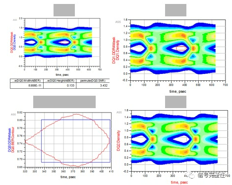
Figure 8 - Test Case #3 - DQ[0-2] - Data rate = 3200 Mbps, MB = 16L PCB, NO VIAS in the channel, Rs = 25, ODT = 240, MB CH Length = 500 mil, Total Channel Length = 937 mils, ALL SIGNALS ON TOP LAYER
Table 6 - Test Case #3 Results
Channel Insertion Loss Analysis
When taking a closer look at the channel insertion loss of Test Case #2, specifically the channels with the 73.1 mil stubs and with the 83.3 mil stub discontinuities, it can be better understood why one simulation passed DDR4 compliance mask requirements. As shown by the insertion loss plots depicted in Figure 9, when comparing the 73.1 mil to 83.3 mil stubs as part of the channel, the overall channel loss from 1.6 GHz to around 9 GHz seems to be fairly similar only differing by a few decibels (dB). Although, the loss seen at 10 GHz, which is close to 6 times the DDR4-3200 clock frequency, increases by 8dB with the 10 mils of additional stub length. This brings the total channel loss to approximately 20dB. Also as shown, the channel with the 73.1 mil stub is resonating at close to 14 GHz, whereas the channel with 83.3 mil stub is resonating at close to 12 GHz. Lastly, there is a 30dB improvement in the channel loss at 12 GHz with 73.1 mil stub versus with the 83.3 mil stubs as part of the channel. This is a significant loss to the channel.
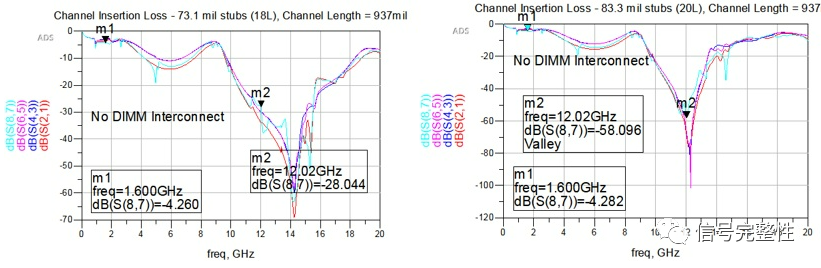
Figure 9 - Test Case #2 - DQ Channel Insertion Loss with 73.1 mil stubs and with 83.3 mil Stubs in Channel
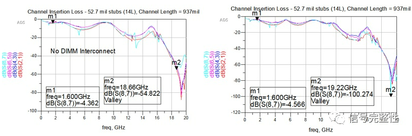
Figure 10 - Test Case #2 (left) vs. Test Case #3 (right) - DQ Channel Insertion Loss without stubs with 52.7 mil stubs in channel
When taking a closer look at the insertion loss for channels with 52.7 mil stubs for both Test Case #2 and Test Case #3, it is not easy to understand why the Test Case #2 channel simulation passed the DDR4 compliance mask requirements and Test Case #3 did not. As shown in Figure 10, the insertion loss plots for both Test Case #2 and #3 channels, the overall channel loss from 1.6 GHz to around 10 GHz seems to remain fairly constant. At 14 GHz, Test Case #3 with 52.7 mil stubs sees a loss that is almost 10dB worse loss than Test Case #2 with the 52.7 mil stubs as part of the channel.
Of course, the channel for Test Case #3 fails due to this 10dB of additional insertion loss. In fact, at this point the total channel loss is close to 30dB. In addition, the resonant frequency of both of these channels is almost the same at about 19 GHz. (This makes sense since the stub length is the same at 52.7 mils for both channels.) The difference is that the resonant frequency for Test Case #3 is exhibiting a much greater loss than Test Case #2 at the channel resonant frequency, in fact by almost 10 dB. This would indicate that the DIMM interconnect is causing this additional 10dB loss to the channel.
DDR4 Channel Eye Diagram Analysis
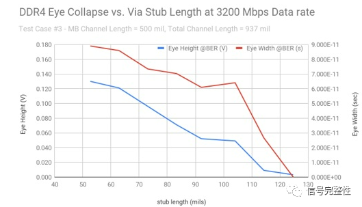
Figure 11 - Test Case #3 - Summary of DDR4 Eye results vs. Stub length with DIMM
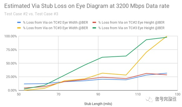
Figure 12 - Estimated Via Stub Loss on Eye Diagram at 32000 Mbps Data Rate with and without DIMM
Now let’s look at some analysis of the eye diagrams for Test Case #2 and Test Case #3. The data from each simulation was tabulated to create these charts shown in Figures 11 and 12. Referring to Figure 12, the max eye diagram loss for test case #2 varies between 2 percent to around 30 percent depending on the stub length in the channel, whereas for Test Case #3, the eye diagram loss reaches almost 100 percent.
Also, as observed in Figure 12, there is an 11.8 percent greater loss in eye height for Test Case #3 versus Test Case #2 with 73.1 mil stubs in the channel. As a reminder, Test Case #2 passed DDR4 compliance eye mask requirements with a 73.1 mil stub as part of the channel. This would indicate that the DIMM interconnect affects the eye height by ~12 percent. For Test Case #2 with 73.1 mil stubs as part of the channel, the loss in the eye height is around 16 percent. For the 83.3 mil stub, the eye height loss only increases slightly to ~20 percent. This would indicate that the eye mask violation occurred in the channel on Test Case #2 from the signal reflections of the 83 mil stub resonating at approximately 12 GHz as well as from the overall channel loss reaching close to 30dB.
Lastly when referring to Figure 11, the JEDEC standard [7] defines the DDR4-3200 DQ receive eye mask as 110 mV peak-to-peak and a timing window of 0.23UI. It can be observed for Test Case #3 that the eye should have passed the DDR4-3200 eye mask with 52 mil stubs as part of the channel; we will explore why it did not in the next section.
DDR4 Channel Analysis Deterministic Jitter Estimates
As shown by Figure 13 when referring to Test Case #2 with the 73.1 mil stubs as part of the channel, there is only 133 ps of margin available. That means 57.44 % of the DDR4 data valid window is consumed by deterministic jitter. As shown by the estimation of the deterministic jitter for Test Case #2 and Test Case #3, both with 52.7 mil stubs as part of the channel, the margin available for a valid data window is very limited. Keep in mind that for DDR4-3200, 1 UI is only 312.5 ps. For Test Case #2 with a 52.7 mil stub as part of the channel, there is an estimated 156.2 ps of deterministic jitter. That is approximately 50 percent of the data valid window for 1 UI being consumed by deterministic jitter! That means when adding the DIMM interconnect as part of the channel, the DDR4 data valid window is consumed by an additional 21 percent from deterministic jitter. This leaves practically no margin available for a valid data window.
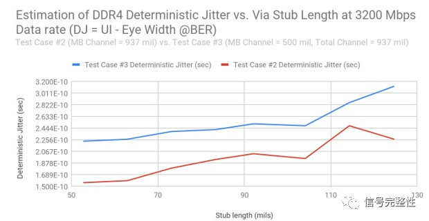
Figure 13 - Deterministic Jitter Estimation vs. Stub length for DDR4 Channel for with and without DIMM
Conclusions
When creating solutions to meet the challenges in the DDR4 channel, you cannot only have signal integrity in mind, since these problems will become even more difficult to solve when power integrity, as well as crosstalk from other signals are added as part of the channel. In other words, to ensure success you need to simulate your own channel design with all the correct models. Analysis showed that without any equalization, the max stub length for DDR4-3200 channel in a point-to-point scenario without any DIMM interconnect is 73.1 mils. Also as shown, these vias will add a significant amount of deterministic jitter to the DDR4 channel.
Due to shrinking UIs there, are multiple other challenges that will need to be accounted for as part of this signal integrity scenario with DDR4. As shown, there was no solution that was found with both vias and DDR4 DIMM interconnect as part of the channel which pass the DDR4-3200 receive eye mask requirements. The DIMM interconnect alone adds enough loss to the channel that must be accounted for, and this will become even more challenging when approaching an SI problem for a 2 DIMM per channel model for DDR4-3200. This shows that simulation with equalization is required to mitigate the effects of the DDR4 DIMM interconnect from deterministic jitter and the overall channel loss.
Without any equalization, eye mask failures will occur even if the discontinuity is resonating at 5 times greater than the Nyquist frequency. That makes this rule of thumb invalid for the DDR4 channel design applications of the future. In other words, the entire channel needs to be designed in detail, and equalization will play a greater role in the future of DDR4.
编辑:黄飞
-
教大家对DDR4做仿真小凡 2022-09-13
-
高速设计:用于DDR3/DDR4的xSignalAltium 2023-06-25
-
DDR4 DESIGN2015-04-24 0
-
MICORN DDR42019-02-18 0
-
DDR3和DDR4在PCB布局设计上的区别2019-03-07 0
-
过孔当道,高速DDR4信号该何去何从?2020-02-28 0
-
DDR4复位偏差要求是什么?2020-08-27 0
-
深圳专业收购DDR42021-01-30 0
-
佛山回收DDR4 高价回收DDR42021-07-15 0
-
DDR4协议规范之(一)DDR4结构和寻址 精选资料推荐2021-07-29 0
-
深圳回收DDR4 收购DDR4内存2021-09-08 0
-
过孔STUB长,DDR信号“强”?2022-05-11 0
-
DDR4,什么是DDR42010-03-24 3174
-
DDR4通道中过孔 stub对信号质量的影响分析2021-03-23 6255
全部0条评论

快来发表一下你的评论吧 !
