

Power Sequencing the MAX14885E VGA Crossover Switch
模拟技术
2285人已加入
描述
The MAX14885E, a fully integrated low-capacitance VGA dual-graphics crossover switch, connects a VGA source to a VGA monitor. This application note explains the proper sequencing of the MAX14885E’s two power supplies, VCC and VL, on power-up.
Introduction
The MAX14885E, a 2:2 VGA switch, connects a VGA source to a VGA monitor. To ease direct connection to graphics controllers or the ASIC, the MAX14885E has two supplies: VCC, a 5V ±5% supply, drives the VGA side interface; and the VL supply sets the logic switching thresholds on the digital input pins (EN, S00, S01, S10, S11, SHA, SHB, SVA, and SVB). This application note documents the proper sequencing of the VCC and VL power supplies on power-up.
Proper Power Sequencing
To ensure that the MAX14885E operates correctly, the VCC and VL supplies must be properly sequenced. It is easiest to understand the correct sequencing conditions if we split the discussion into two cases: first, when VL rises before (or coincidently) with VCC; and second, the case when VL rises after VCC.
Case 1: When VL Rises Before VCC
The MAX14885E powers up properly when VL rises before VCC rises or when it rises coincidently with VCC. This is shown inFigures 1 and 2.
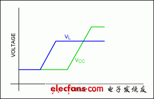
Figure 1. VL rises in advance of the VCC rising, resulting in a good power-up.
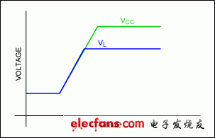
Figure 2. VL rises coincidently with the VCC rising, resulting in a good power-up.
Case 2: When VL Rises After VCC
In the situation where VL starts rising after VCC begins to rise at power-up, some care must be taken (Figure 3). For proper power-up, users must ensure that VCC has settled before VL starts rising.
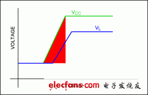
Figure 3. VL rises too soon after VCC, resulting in a bad power-up.
VL needs to start rising after VCC has settled (outside of the red triangle illustrated in Figure 4).
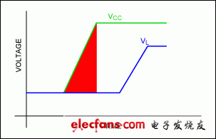
Figure 4. VL rises after VCC has settled, resulting in a good power-up.
To provide a safety margin against variations in production and sequencing external power-supply circuits, it is recommended that the delay from VCC rising to VL rising be at least twice the rise time of the VCC supply.
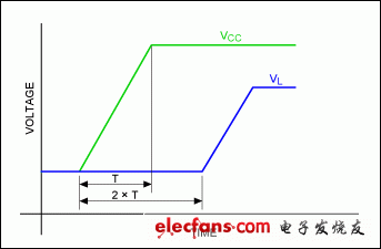
Figure 5. Definition and requirements for safe timing with margin.
Detailed Analysis of Power Sequencing
Often, power supply rails rise as shown in the previous figures. In some cases, however, the point where a power-supply transition ends is not so clear. This section describes a quantitative means to analyze a given specific scenario where VL rises after VCC. This method ensures that there is sufficient delay for correct power-up sequencing.
To determine this, four time measurements must be taken. Two of these measurements are with respect to specific voltage levels on VCC, and the other two are with respect to specific voltage levels on VL. All four measurements are to be taken from a single scope capture.
The following time measurements need to be taken:
- TVCC90 = the time at which the VCC rising waveform has reached 90% of its final value, which should be 90% of 5V.
- TVCC10 = the time at which the VCC rising waveform has reached 10% of its final value, which should be 10% of 5V.
- TVL90 = the time at which the VL rising waveform has reached 90% of its final value, which will be 90% of 3.3V or 90% of 2.5V.
- TVL10 = the time at which the VL rising waveform has reached 10% of its final value, which will be 10% of 3.3V or 10% of 2.5V.
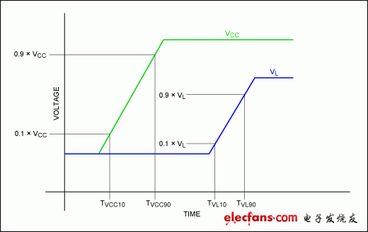
Figure 6. The time measurements needed to analyze a scenario where VL rises after VCC.
Now, perform the following calculations:

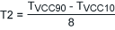
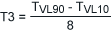
To ensure sufficient margin between VCC and VL rising at power-up, the external power supply design must guarantee that:

Conclusion
This application note has described the correct power-up conditions for the MAX14885E VGA dual-graphics crossover switch. It has recommended how much margin to use in the sequencing delay if VL succeeds VCC when powering up. It has also provided a set of calculations to use when the trailing edge of the power supply ramp is not clearly defined.
声明:本文内容及配图由入驻作者撰写或者入驻合作网站授权转载。文章观点仅代表作者本人,不代表电子发烧友网立场。文章及其配图仅供工程师学习之用,如有内容侵权或者其他违规问题,请联系本站处理。
举报投诉
-
SWITCH POWER SUPPLY DESIGN2012-08-16 0
-
使用MAX14983E制作VGA切换器,不闪屏!2016-06-26 0
-
使用“power_mode_switch_rtos”关闭MCU时系统卡住了怎么解决?2023-03-30 0
-
Switching VGA Signals in a Not2009-04-20 703
-
MAX4885E Fully Integrated VGA2009-04-22 1033
-
Sequencing with the MAX16046 S2009-11-16 1199
-
MAX14885E 低电容VGA 2:2双通道图形交叉点开关2010-04-10 630
-
MAX14885E 完全集成的VGA交叉点开关,具有宽带和增2010-05-06 1868
-
MAX14885E VGA交叉开关电源排序2012-01-31 643
-
MAX14885E VGA 交叉开关的电源排序2022-11-17 47
-
MAX14885E VGA交越开关的电源排序2023-01-11 445
-
MAX16895-MAX16899: Ultra-Small, High Accuracy, Adjustable Sequencing/Supervisory Circuits Data Sheet MAX16895-MAX16899: Ultra-Small, High Ac2023-10-13 9
全部0条评论

快来发表一下你的评论吧 !
