
资料下载


负空间应用设计:PC板电源设计的数字控制技术
分享资料个
负空间应用设计:PC板电源设计的数字控制技术
越来越多的处理到网络和计算设备的印刷电路板(PCB)始终是一个“处理能力与权力”悖论。较新的集成电路(IC)的设计包多次处理能力在同一空间超过上一代设备。这种增加的能力使高性能的产品,如一个软件定义的网络(SDN)开关与额外的开关能力或自动化测试设备(ATE)设备具有更快的吞吐量。然而,更高的处理能力也可能意味着更高的功率要求,与IC和电源模块使用更多的PCB房地产
How can designers recover board space lost to rising power requirements fueled by the need for increased processing capability? At GE we look at solutions to these challenges with a principle we call Designing in the Negative Space.
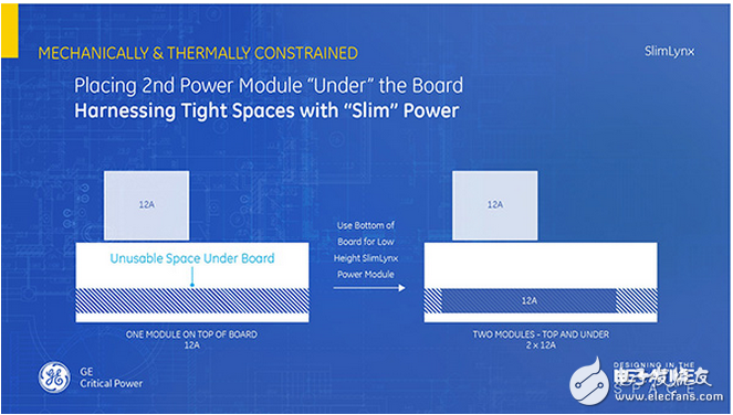
Designing in the Negative Space (DITNS) looks at a number of engineering approaches to reduce the power module “footprint” on a printed circuit board. For example, making power modules denser while reducing their height enables designers to place them in previously unusable spaces. We see this approach used with GE’s low-height SlimLynx™ family of point-of-load (POL), or DC/DC converter, power modules that fit under a mezzanine board, or that can be placed on the back of the board, freeing up top-of-board space for taller components. (See Figure 1)

声明:本文内容及配图由入驻作者撰写或者入驻合作网站授权转载。文章观点仅代表作者本人,不代表电子发烧友网立场。文章及其配图仅供工程师学习之用,如有内容侵权或者其他违规问题,请联系本站处理。 举报投诉
- 相关下载
- 相关文章


