
资料下载


通信应用微分电路设计技术
分享资料个
通信应用微分电路设计技术
在通信系统设计的主要挑战之一是成功捕获信号具有足够的保真度。严格的标准规范要求适当的接口拓扑选择。部署蜂窝电话的通信标准,如码分多址(CDMA)和宽带CDMA,需要高动态范围,高输入线性度和低噪声,以避免阻断剂的影响,信号失真,和灵敏度退化。在过去,完全差分信号链的性能优势是捏造的单端选项,由于实际应用问题。然而,集成RF电路技术和可扩展的高性能差分RF积木的最新进展允许差分架构,以适用于高性能接收机设计。
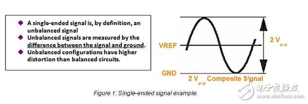
A single-ended signal is unbalanced by definition and is measured by the difference between the signal of interest and a constant reference point, normally ground, which serves as the return path for the signal. A problem can be encountered if an error source is introduced to the single-ended signal. Since the ground reference will be unaffected by the injected error, the error is carried forward through the signal. In a single-ended configuration, any variation introduced to the desired signal will be problematic to remove without involving overly complex cancellation techniques. For this reason, single-ended or unbalanced signals are more prone to noise and interference, such as electro-magnetic coupled interference. Also, as will be shown later, unbalanced configurations have higher distortion than balanced circuits.

声明:本文内容及配图由入驻作者撰写或者入驻合作网站授权转载。文章观点仅代表作者本人,不代表电子发烧友网立场。文章及其配图仅供工程师学习之用,如有内容侵权或者其他违规问题,请联系本站处理。 举报投诉
- 相关下载
- 相关文章


