
资料下载


ad9865宽带调制解调器混合信号前端数据表
分享资料个
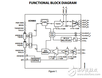
The AD9865 is a mixed-signal front end (MxFE) IC for transceiver applications requiring Tx and Rx path functionality with data rates up to 80 MSPS. Its flexible digital interface, power saving modes, and high Tx-to-Rx isolation make it well suited for half- and full-duplex applications. The digital interface is extremely flexible allowing simple interfaces to digital back ends that support half- or full-duplex data transfers, thus often allowing the AD9865 to replace discrete ADC and DAC solutions. Power saving modes include the ability to reduce power consumption of individual functional blocks, or to power down unused blocks in half-duplex applications. A serial port interface (SPI®) allows software programming of the various functional blocks. An on-chip PLL clock multiplier and synthesizer provide all the required internal clocks, as well as two external clocks from a single crystal or clock source. The Tx signal path consists of a bypassable 2×/4× low-pass interpolation filter, a 10-bit TxDAC, and a line driver. The transmit path signal bandwidth can be as high as 34 MHz at an input data rate of 80 MSPS. The TxDAC provides differential current outputs that can be steered directly to an external load or to an internal low distortion current amplifier. The current amplifier (IAMP) can be configured as a current- or voltagemode line driver (with two external npn transistors) capable of delivering in excess of 23 dBm peak signal power. Tx power can be digitally controlled over a 19.5 dB range in 0.5 dB steps. The receive path consists of a programmable amplifier (RxPGA), a tunable low-pass filter (LPF), and a 10-bit ADC. The low noise RxPGA has a programmable gain range of −12 dB to +48 dB in 1 dB steps. Its input referred noise is less than 3 nV/rtHz for gain settings beyond 36 dB. The receive path LPF cutoff frequency can be set over a 15 MHz to 35 MHz range or simply bypassed. The 10-bit ADC achieves excellent dynamic performance over a 5 MSPS to 80 MSPS span. Both the RxPGA and the ADC offer scalable power consumption allowing power/performance optimization. The AD9865 provides a highly integrated solution for many broadband modems. It is available in a space saving 64-pin chip scale package and is specified over the commercial (−40°C to +85°C) temperature range.

声明:本文内容及配图由入驻作者撰写或者入驻合作网站授权转载。文章观点仅代表作者本人,不代表电子发烧友网立场。文章及其配图仅供工程师学习之用,如有内容侵权或者其他违规问题,请联系本站处理。 举报投诉
- 相关下载
- 相关文章


