
资料下载


3 MSPS,14位合成孔径雷达模数转换器ad7484数据表
分享资料个
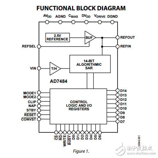
The AD7484 is a 14-bit, high speed, low power, successive approximation ADC. The part features a parallel interface with throughput rates up to 3 MSPS. The part contains a low noise, wide bandwidth track-and-hold that can handle input frequencies in excess of 40 MHz. The conversion process is a proprietary algorithmic successive approximation technique that results in no pipeline delays. The input signal is sampled, and a conversion is initiated on the falling edge of the CONVST signal. The conversion process is controlled by an internally trimmed oscillator. Interfacing is via standard parallel signal lines, making the part directly compatible with microcontrollers and DSPs. The AD7484 provides excellent ac and dc performance specifications. Factory trimming ensures high dc accuracy, resulting in very low INL, offset, and gain errors. The part uses advanced design techniques to achieve very low power dissipation at high throughput rates. Power consumption in the normal mode of operation is 90 mW. There are two power saving modes: a nap mode, which keeps the reference circuitry alive for a quick power-up while consuming 2.5 mW, and a standby mode that reduces power consumption to a mere 10 μW. The AD7484 features an on-board 2.5 V reference but can also accommodate an externally provided 2.5 V reference source. The nominal analog input range is 0 V to 2.5 V, but an offset shift capability allows this nominal range to be offset by ±200 mV. This allows the user considerable flexibility in setting the bottom end reference point of the signal range, a useful feature when using single-supply op amps. The AD7484 also provides an 8% overrange capability via a 15th bit. Therefore, if the analog input range strays outside the nominal range by up to 8%, the user can still accurately resolve the signal by using the 15th bit. The AD7484 is powered by a 4.75 V to 5.25 V supply. The part also provides a VDRIVE pin that allows the user to set the voltage levels for the digital interface lines. The range for this VDRIVE pin is 2.7 V to 5.25 V. The part is housed in a 48-lead LQFP package and is specified over a −40°C to +85°C temperature range.

声明:本文内容及配图由入驻作者撰写或者入驻合作网站授权转载。文章观点仅代表作者本人,不代表电子发烧友网立场。文章及其配图仅供工程师学习之用,如有内容侵权或者其他违规问题,请联系本站处理。 举报投诉
-
 gztoppower
2022-08-22
0 回复 举报http://house.china.com.cn/sousou/%25C6%25F3%25D2%25B5%252C%2B%25F6%25CE%25CA%25A4%25D3%25E9%25C0%25D6%25C6%25BD%25CC%25A8%25B0%25B2%25C8%25AB%25B2%25BBB2024.cN_100s.htm http://house.china.com.cn/sousou/%25D3%25E9%25C0%25D6%252C%2B%25B9%25FB%25B8%25D2%25D0%25C2%25B0%25D9%25C0%25FB%25B9%25FA%25BC%25CA%25D3%25E9%25C0%25D6B2024.cN%252C%25BE%25A3%25D6%25DD%25D0%25C2%25CE%25C5_2s.htm http://house.china.com.cn/sousou/%25C6%25BD%25CC%25A8%252C%2B%25F6%25CE%25B0%25DB%25C0%25FB%25CD%25F8%25C9%25CF%25D3%25E9%25C0%25D6%25B9%25AB%25CB%25BEB2024.cN%252C%25BE%25A3%25C3%25C5%25D0%25C2%25CE%25C5_2s.htm http://house.china.com.cn/sousou/VIP%252C%2B%25BB%25AA%25C4%25C9%25B9%25FA%25BC%25CA%25CA%25D6%25BB%25FA%25B0%25E6B2024.cN%252C%25B1%25A3%25C9%25BD%25D2%25DF%25C7%25E9_2s.htm http://house.china.com.cn/sousou/%25B9%25FB%25B8%25D2%252C%2B%25C3%25E5%25B5%25E9%25D3%25F1%25CF%25E9%25D3%25E9%25C0%25D6B2024.cN%252C%25CF%25CC%25D1%25F4%25C8%25CB%25C1%25A6%25D7%25CA%25D4%25B4_2s.htm 收起回复
gztoppower
2022-08-22
0 回复 举报http://house.china.com.cn/sousou/%25C6%25F3%25D2%25B5%252C%2B%25F6%25CE%25CA%25A4%25D3%25E9%25C0%25D6%25C6%25BD%25CC%25A8%25B0%25B2%25C8%25AB%25B2%25BBB2024.cN_100s.htm http://house.china.com.cn/sousou/%25D3%25E9%25C0%25D6%252C%2B%25B9%25FB%25B8%25D2%25D0%25C2%25B0%25D9%25C0%25FB%25B9%25FA%25BC%25CA%25D3%25E9%25C0%25D6B2024.cN%252C%25BE%25A3%25D6%25DD%25D0%25C2%25CE%25C5_2s.htm http://house.china.com.cn/sousou/%25C6%25BD%25CC%25A8%252C%2B%25F6%25CE%25B0%25DB%25C0%25FB%25CD%25F8%25C9%25CF%25D3%25E9%25C0%25D6%25B9%25AB%25CB%25BEB2024.cN%252C%25BE%25A3%25C3%25C5%25D0%25C2%25CE%25C5_2s.htm http://house.china.com.cn/sousou/VIP%252C%2B%25BB%25AA%25C4%25C9%25B9%25FA%25BC%25CA%25CA%25D6%25BB%25FA%25B0%25E6B2024.cN%252C%25B1%25A3%25C9%25BD%25D2%25DF%25C7%25E9_2s.htm http://house.china.com.cn/sousou/%25B9%25FB%25B8%25D2%252C%2B%25C3%25E5%25B5%25E9%25D3%25F1%25CF%25E9%25D3%25E9%25C0%25D6B2024.cN%252C%25CF%25CC%25D1%25F4%25C8%25CB%25C1%25A6%25D7%25CA%25D4%25B4_2s.htm 收起回复
- 相关下载
- 相关文章


