
资料下载


1.2千兆赫时钟分配IC锁相环核心分频器延迟调整五输出ad9511数据表
分享资料个
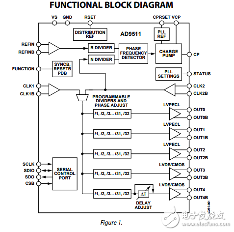
The AD9511 provides a multi-output clock distribution function along with an on-chip PLL core. The design emphasizes low jitter and phase noise to maximize data converter performance. Other applications with demanding phase noise and jitter requirements also benefit from this part. The PLL section consists of a programmable reference divider (R); a low noise phase frequency detector (PFD); a precision charge pump (CP); and a programmable feedback divider (N)。 By connecting an external VCXO or VCO to the CLK2/CLK2B pins, frequencies up to 1.6 GHz may be synchronized to the input reference. There are five independent clock outputs. Three outputs are LVPECL (1.2 GHz), and two are selectable as either LVDS (800 MHz) or CMOS (250 MHz) levels. Each output has a programmable divider that may be bypassed or set to divide by any integer up to 32. The phase of one clock output relative to another clock output may be varied by means of a divider phase select function that serves as a coarse timing adjustment. One of the LVDS/CMOS outputs features a programmable delay element with full-scale ranges up to 10 ns of delay. This fine tuning delay block has 5-bit resolution, giving 32 possible delays from which to choose for each full-scale setting. The AD9511 is ideally suited for data converter clocking applications where maximum converter performance is achieved by encode signals with subpicosecond jitter. The AD9511 is available in a 48-lead LFCSP and can be operated from a single 3.3 V supply. An external VCO, which requires an extended voltage range, can be accommodated by connecting the charge pump supply (VCP) to 5.5 V. The temperature range is −40°C to +85°C.

声明:本文内容及配图由入驻作者撰写或者入驻合作网站授权转载。文章观点仅代表作者本人,不代表电子发烧友网立场。文章及其配图仅供工程师学习之用,如有内容侵权或者其他违规问题,请联系本站处理。 举报投诉
- 相关下载
- 相关文章


