
资料下载


1.6千兆赫时钟分配IC分频器延迟调整两个输出ad9515数据表
分享资料个
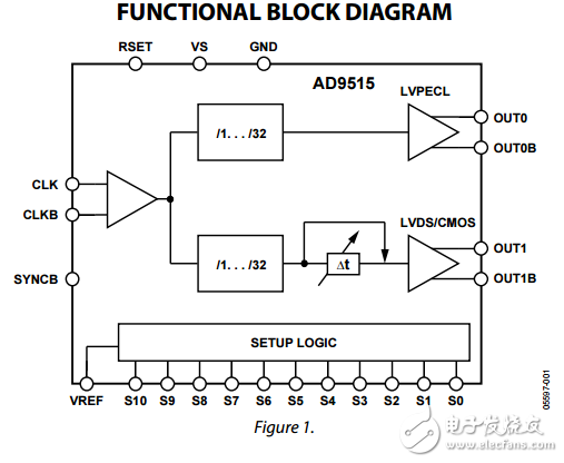
The AD9515 features a two-output clock distribution IC in a design that emphasizes low jitter and phase noise to maximize data converter performance. Other applications with demanding phase noise and jitter requirements also benefit from this part. There are two independent clock outputs. One output is LVPECL, while the other output can be set to either LVDS or CMOS levels. The LVPECL output operates to 1.6 GHz. The other output operates to 800 MHz in LVDS mode and to 250 MHz in CMOS mode. Each output has a programmable divider that can be set to divide by a selected set of integers ranging from 1 to 32. The phase of one clock output relative to the other clock output can be set by means of a divider phase select function that serves as a coarse timing adjustment. The LVDS/CMOS output features a delay element with three selectable full-scale delay values (1.5 ns, 5 ns, and 10 ns), each with 16 steps of fine adjustment. The AD9515 does not require an external controller for operation or setup. The device is programmed by means of 11 pins (S0 to S10) using 4-level logic. The programming pins are internally biased to ⅓ VS. The VREF pin provides a level of ⅔ VS. VS (3.3 V) and GND (0 V) provide the other two logic levels. The AD9515 is ideally suited for data converter clocking applications where maximum converter performance is achieved by encode signals with subpicosecond jitter. The AD9515 is available in a 32-lead LFCSP and operates from a single 3.3 V supply. The temperature range is −40°C to +85°C.

声明:本文内容及配图由入驻作者撰写或者入驻合作网站授权转载。文章观点仅代表作者本人,不代表电子发烧友网立场。文章及其配图仅供工程师学习之用,如有内容侵权或者其他违规问题,请联系本站处理。 举报投诉
- 相关下载
- 相关文章


