
资料下载


CMOS,180兆赫数字频率合成器AD9851数据表
分享资料个
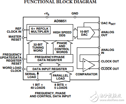
The AD9851 is a highly integrated device that uses advanced DDS technology, coupled with an internal high speed, high performance D/A converter, and comparator, to form a dig i tal ly programmable frequency synthesizer and clock generator func- tion. When referenced to an accurate clock source, the AD9851 generates a stable frequency and phase-programmable digitized analog output sine wave. This sine wave can be used directly as a frequency source, or internally converted to a square wave for agile-clock generator applications. The AD9851’s innovative high speed DDS core accepts a 32-bit frequency tuning word, which results in an output tuning res o lu tion of approximately 0.04 Hz with a 180 MHz system clock. The AD9851 con tains a unique 6 REFCLK Multiplier circuit that eliminates the need for a high speed reference oscillator. The 6 REFCLK Multiplier has min i mal impact on SFDR and phase noise char- ac ter is tics. The AD9851 provides fi ve bits of programmable phase mod u la tion resolution to enable phase shifting of its output in in cre ments of 11.25°。 The AD9851 contains an internal high speed comparator that can be confi gured to accept the (externally) fi ltered output of the DAC to generate a low jitter output pulse. The frequency tuning, control, and phase modulation words are asynchronously loaded into the AD9851 via a parallel or serial loading format. The parallel load format consists of fi ve it er a tive loads of an 8-bit control word (byte)。 The fi rst 8-bit byte controls output phase, 6 REFCLK Multiplier, power-down enable and loading for mat; the remaining bytes comprise the 32-bit frequency tuning word. Serial loading is accomplished via a 40-bit serial data stream entering through one of the parallel input bus lines. The AD9851 uses advanced CMOS technology to provide this break- through level of functionality on just 555 mW of power dissipation (5 V supply), at the maximum clock rate of 180 MHz. The AD9851 is available in a space-saving 28-lead SSOP, surface-mount package that is pin-for-pin compatible with the popular AD9850 125 MHz DDS. It is specifi ed to operate over the extended industrial temperature range of –40°C to +85°C at 》3.0 V supply voltage. Below 3.0 V, the specifi cations apply over the commercial temperature range of 0°C to 85°C.

声明:本文内容及配图由入驻作者撰写或者入驻合作网站授权转载。文章观点仅代表作者本人,不代表电子发烧友网立场。文章及其配图仅供工程师学习之用,如有内容侵权或者其他违规问题,请联系本站处理。 举报投诉
- 相关下载
- 相关文章


