
资料下载


1.8V,12-lvds/24-cmos输出低功耗时钟扇出缓冲器adclk854数据表
分享资料个
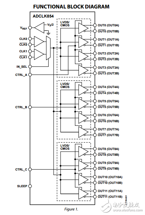
The ADCLK854 is a 1.2 GHz/250 MHz LVDS/CMOS fanout buffer optimized for low jitter and low power operation. Possible configurations range from 12 LVDS to 24 CMOS outputs, including combinations of LVDS and CMOS outputs. Three control lines are used to determine whether fixed blocks of outputs (three banks of four) are LVDS or CMOS outputs. The ADCLK854 offers two selectable inputs and a sleep mode feature. The IN_SEL pin state determines which input is fanned out to all the outputs. The SLEEP pin enables a sleep mode to power down the device. The inputs accept various types of single-ended and differential logic levels including LVPECL, LVDS, HSTL, CML, and CMOS. Table 8 provides interface options for each type of connection. This device is available in a 48-pin LFCSP package. It is specified for operation over the standard industrial temperature range of −40°C to +85°C.

声明:本文内容及配图由入驻作者撰写或者入驻合作网站授权转载。文章观点仅代表作者本人,不代表电子发烧友网立场。文章及其配图仅供工程师学习之用,如有内容侵权或者其他违规问题,请联系本站处理。 举报投诉
- 相关下载
- 相关文章


