
资料下载


超快SiGe集电极开路HVDS时钟/数据缓冲区adclk914数据表
分享资料个
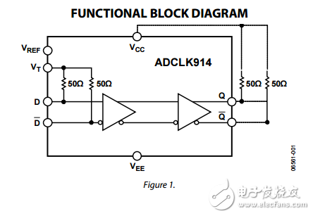
The ADCLK914 is an ultrafast clock/data buffer fabricated on the Analog Devices, Inc., proprietary, complementary bipolar (XFCB-3) silicon-germanium (SiGe) process. The ADCLK914 features high voltage differential signaling (HVDS) outputs suitable for driving the latest Analog Devices high speed digitalto-analog converters (DACs)。 The ADCLK914 has a single, differential open-collector output. The ADCLK914 buffer operates up to 7.5 GHz with a 160 ps propagation delay and adds only 110 fs random jitter (RJ)。 The input has a center tapped, 100 Ω, on-chip termination resistor and accepts LVPECL, CML, CMOS, LVTTL, or LVDS (ac-coupled only)。 A VREF pin is available for biasing ac-coupled inputs. The HVDS output stage is designed to directly drive 1.9 V each side into 50 Ω terminated to VCC for a total differential output swing of 3.8 V. The ADCLK914 is available in a 16-lead LFCSP. It is specified for operation over the extended industrial temperature range of −40°C to +125°C.

声明:本文内容及配图由入驻作者撰写或者入驻合作网站授权转载。文章观点仅代表作者本人,不代表电子发烧友网立场。文章及其配图仅供工程师学习之用,如有内容侵权或者其他违规问题,请联系本站处理。 举报投诉
- 相关下载
- 相关文章


