
资料下载


5伏3A逻辑控制高侧或低侧负载开关ADP1196数据表
分享资料个
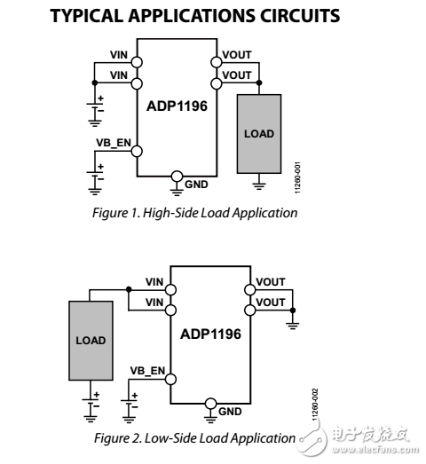
The ADP1196 is a high-side or low-side load switch designed for VIN operation between 0 V and 5.5 V with a VB_EN supply of 1.83 V to 5.5 V. The device contains an internal charge pump that operates from either VIN or VB_EN, whichever is higher, and an ultralow on resistance, N-channel MOSFET. This N-channel MOSFET supports more than 2 A of continuous current at VIN close to 0 V, and, with its ultralow on resistance, minimizes power loss. In addition, the on resistance is constant, independent of the VIN or VB_EN voltage. The low 26 µA quiescent current and ultralow shutdown current make the ADP1196 ideal for low power applications.
When the junction temperature exceeds 125°C, overtemperature protection circuitry is activated, thereby protecting the ADP1196 and downstream circuits from potential damage.
The ADP1196 occupies minimal printed circuit board (PCB) space, with an area of less than 1.5 mm2 and a height of 0.60 mm.
The ADP1196 is available in an ultrasmall 1.0 mm × 1.5 mm, 6-ball, 0.5 mm pitch WLCSP.

声明:本文内容及配图由入驻作者撰写或者入驻合作网站授权转载。文章观点仅代表作者本人,不代表电子发烧友网立场。文章及其配图仅供工程师学习之用,如有内容侵权或者其他违规问题,请联系本站处理。 举报投诉
- 相关下载
- 相关文章


