
资料下载


×
实例解析FPGA和单片机的串行通信接口设计
消耗积分:1 |
格式:rar |
大小:0.6 MB |
2017-11-01
分享资料个
现场可编程逻辑器件(FPGA)在高速采集系统中的应用越来越广,由于FPGA对采集到的数据的处理能力比较差,故需要将其采集到的数据送到其他CPU系统来实现数据的处理功能,这就使FPGA系统与其他CPU系统之间的数据通信提到日程上,得到人们的急切关注。本文介绍利用VHDL语言实现 FPGA与单片机的串口异步通信电路。
整个设计采用模块化的设计思想,可分为四个模块:FPGA数据发送模块,FPGA波特率发生控制模块,FPGA总体接口模块以及单片机数据接收模块。本文着重对FPGA数据发送模块实现进行说明。
2 FPGA数据发送模块的设计
根据RS232 异步串行通信来的帧格式,在FPGA发送模块中采用的每一帧格式为:1位开始位+8位数据位+1位奇校验位+1位停止位,波特率为2400。本系统设计的是将一个16位的数据封装成高位帧和低位帧两个帧进行发送,先发送低位帧,再发送高位帧,在传输数据时,加上文件头和数据长度,文件头用555555来表示,只有单片机收到555555时,才将下面传输的数据长度和数据位进行接收,并进行奇校验位的检验,正确就对收到的数据进行存储处理功能,数据长度可以根据需要任意改变。由设置的波特率可以算出分频系数,具体算法为分频系数X=CLK/(BOUND*2)。可由此式算出所需的任意波特率。下面是实现上述功能的VHDL源程序。
Library ieee;
use ieee.std_logic_1164.all;
use ieee.std_logic_arith.all;
use ieee.std_logic_unsigned.all;
entity atel2_bin is
port( txclk: in std_logic; --2400Hz的波特率时钟
reset: in std_logic; --复位信号
din: in std_logic_vector(15 downto 0); --发送的数据
start: in std_logic; --允许传输信号
sout: out std_logic --串行输出端口
);
end atel2_bin;
architecture behav of atel2_bin is
signal thr,len: std_logic_vector(15 downto 0);
signal txcnt_r: std_logic_vector(2 downto 0);
signal sout1: std_logic;
signal cou: integer:=0;
signal oddb:std_logic;
type s is(start1,start2,shift1,shift2,odd1,odd2,stop1,stop2);
signal state:s:=start1;
begin
process(txclk)
begin
if rising_edge(txclk) then
if cou《3 then thr《=“0000000001010101”; --发送的文件头
elsif cou=3 then
thr《=“0000000000000010”; --发送的文件长度
elsif (cou》3 and state=stop2) then thr《=din;--发送的数据
end if;
end if;
end process;
process(reset,txclk)
variable tsr,tsr1,oddb1,oddb2: std_logic_vector(7 downto 0);
begin
if reset=‘1’ then
txcnt_r《=(others=》‘0’);
sout1《=‘1’;
state《=start1;
cou《=0;
elsif txclk’event and txclk=‘1’ then
case state is
when start1=》
if start=‘1’ then
if cou=3 then
len《=thr;
end if;
tsr:=thr(7 downto 0);
oddb1:=thr(7 downto 0);
sout1《=‘0’; --起始位
txcnt_r《=(others=》‘0’);
state《=shift1;
else
state《=start1;
end if;
when shift1=》
oddb《=oddb1(7) xor oddb1(6) xor oddb1(5) xor oddb1(4) xor oddb1(3) xor oddb1(2) xor oddb1(1) xor oddb1(0);
sout1《=tsr(0); --数据位
tsr(6 downto 0):=tsr(7 downto 1);
tsr(7):=‘0’;
txcnt_r《=txcnt_r+1;
if (txcnt_r=7) then
state《=odd1;cou《=cou+1;
end if;
when odd1=》 --奇校验位
if oddb=‘1’ then
sout1《=‘0’;state《=stop1;
else
sout1《=‘1’;state《=stop1;
end if;
when stop1=》
sout1《=‘1’; --停止位
if cou《4 then
state《=start1;
else
state《=start2;
end if;
when start2=》
tsr1:=thr(15 downto 8);
oddb2:=thr(15 downto 8);
sout1《=‘0’; --起始位
txcnt_r《=(others=》‘0’);
state《=shift2;
when shift2=》
oddb《=oddb2(7) xor oddb2(6) xor oddb2(5) xor oddb2(4) xor oddb2(3) xor oddb2(2) xor oddb2(1) xor oddb2(0);
sout1《=tsr1(0);--数据位
tsr1(6 downto 0):=tsr1(7 downto 1);
tsr1(7):=‘0’;
txcnt_r《=txcnt_r+1;
if (txcnt_r=7) then
state《=odd2;
end if;
when odd2=》 --奇校验位
if oddb=‘1’ then
sout1《=‘0’;state《=stop2;
else
sout1《=‘1’;state《=stop2;
end if;
when stop2=》
sout1《=‘1’; --停止位
if len=“0000000000000000” then
state《=stop2;
else
state《=start1;
len《=len-1;
end if;
end case;
end if;
end process;
sout《=sout1;
end behav; 其中各信号的说明已在程序中标明了。波形仿真图如图1所示。
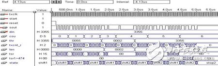
图1 FPGA数据发送时序仿真图
图中Din写入值为3355H,波特率为2400Hz,Start信号始终置逻辑1,即随时都能发送数据。Reset信号逻辑1时复位,逻辑0时电路开始工作。THR是数据寄存器,文件头、数据长度以及数据位都先寄存到THR中,Len是数据长度,TSR是低8位数据帧寄存器,TSR1是高8位数据帧寄存器。数据长度Len定为02H,发送时先发送低8位55H,后发送高8位33H,一共发送两遍。发送的数据格式说明:当发送55H时,其二进制为01010101,则发送的数据的二进制数为00101010111(1位开始位+8位数据位+1位奇校验位+1位停止位)。
单片机部分先对FPGA发送过来的文件头进行确认,正确就接收文件,否则放弃接收的数据。根据FPGA发送模块的协议,对串口控制寄存器SCON和波特率控制寄存器PCON的设置即可实现。
3 总结
目前电子产品的开发中经常要综合运用EDA技术、计算机控制技术、数字信号处理技术,那么电路各部分经常需要数据交换。本文也是基于此给出这方面应用的实例,供开发者交流。
整个设计采用模块化的设计思想,可分为四个模块:FPGA数据发送模块,FPGA波特率发生控制模块,FPGA总体接口模块以及单片机数据接收模块。本文着重对FPGA数据发送模块实现进行说明。
2 FPGA数据发送模块的设计
根据RS232 异步串行通信来的帧格式,在FPGA发送模块中采用的每一帧格式为:1位开始位+8位数据位+1位奇校验位+1位停止位,波特率为2400。本系统设计的是将一个16位的数据封装成高位帧和低位帧两个帧进行发送,先发送低位帧,再发送高位帧,在传输数据时,加上文件头和数据长度,文件头用555555来表示,只有单片机收到555555时,才将下面传输的数据长度和数据位进行接收,并进行奇校验位的检验,正确就对收到的数据进行存储处理功能,数据长度可以根据需要任意改变。由设置的波特率可以算出分频系数,具体算法为分频系数X=CLK/(BOUND*2)。可由此式算出所需的任意波特率。下面是实现上述功能的VHDL源程序。
Library ieee;
use ieee.std_logic_1164.all;
use ieee.std_logic_arith.all;
use ieee.std_logic_unsigned.all;
entity atel2_bin is
port( txclk: in std_logic; --2400Hz的波特率时钟
reset: in std_logic; --复位信号
din: in std_logic_vector(15 downto 0); --发送的数据
start: in std_logic; --允许传输信号
sout: out std_logic --串行输出端口
);
end atel2_bin;
architecture behav of atel2_bin is
signal thr,len: std_logic_vector(15 downto 0);
signal txcnt_r: std_logic_vector(2 downto 0);
signal sout1: std_logic;
signal cou: integer:=0;
signal oddb:std_logic;
type s is(start1,start2,shift1,shift2,odd1,odd2,stop1,stop2);
signal state:s:=start1;
begin
process(txclk)
begin
if rising_edge(txclk) then
if cou《3 then thr《=“0000000001010101”; --发送的文件头
elsif cou=3 then
thr《=“0000000000000010”; --发送的文件长度
elsif (cou》3 and state=stop2) then thr《=din;--发送的数据
end if;
end if;
end process;
process(reset,txclk)
variable tsr,tsr1,oddb1,oddb2: std_logic_vector(7 downto 0);
begin
if reset=‘1’ then
txcnt_r《=(others=》‘0’);
sout1《=‘1’;
state《=start1;
cou《=0;
elsif txclk’event and txclk=‘1’ then
case state is
when start1=》
if start=‘1’ then
if cou=3 then
len《=thr;
end if;
tsr:=thr(7 downto 0);
oddb1:=thr(7 downto 0);
sout1《=‘0’; --起始位
txcnt_r《=(others=》‘0’);
state《=shift1;
else
state《=start1;
end if;
when shift1=》
oddb《=oddb1(7) xor oddb1(6) xor oddb1(5) xor oddb1(4) xor oddb1(3) xor oddb1(2) xor oddb1(1) xor oddb1(0);
sout1《=tsr(0); --数据位
tsr(6 downto 0):=tsr(7 downto 1);
tsr(7):=‘0’;
txcnt_r《=txcnt_r+1;
if (txcnt_r=7) then
state《=odd1;cou《=cou+1;
end if;
when odd1=》 --奇校验位
if oddb=‘1’ then
sout1《=‘0’;state《=stop1;
else
sout1《=‘1’;state《=stop1;
end if;
when stop1=》
sout1《=‘1’; --停止位
if cou《4 then
state《=start1;
else
state《=start2;
end if;
when start2=》
tsr1:=thr(15 downto 8);
oddb2:=thr(15 downto 8);
sout1《=‘0’; --起始位
txcnt_r《=(others=》‘0’);
state《=shift2;
when shift2=》
oddb《=oddb2(7) xor oddb2(6) xor oddb2(5) xor oddb2(4) xor oddb2(3) xor oddb2(2) xor oddb2(1) xor oddb2(0);
sout1《=tsr1(0);--数据位
tsr1(6 downto 0):=tsr1(7 downto 1);
tsr1(7):=‘0’;
txcnt_r《=txcnt_r+1;
if (txcnt_r=7) then
state《=odd2;
end if;
when odd2=》 --奇校验位
if oddb=‘1’ then
sout1《=‘0’;state《=stop2;
else
sout1《=‘1’;state《=stop2;
end if;
when stop2=》
sout1《=‘1’; --停止位
if len=“0000000000000000” then
state《=stop2;
else
state《=start1;
len《=len-1;
end if;
end case;
end if;
end process;
sout《=sout1;
end behav; 其中各信号的说明已在程序中标明了。波形仿真图如图1所示。
图1 FPGA数据发送时序仿真图
图中Din写入值为3355H,波特率为2400Hz,Start信号始终置逻辑1,即随时都能发送数据。Reset信号逻辑1时复位,逻辑0时电路开始工作。THR是数据寄存器,文件头、数据长度以及数据位都先寄存到THR中,Len是数据长度,TSR是低8位数据帧寄存器,TSR1是高8位数据帧寄存器。数据长度Len定为02H,发送时先发送低8位55H,后发送高8位33H,一共发送两遍。发送的数据格式说明:当发送55H时,其二进制为01010101,则发送的数据的二进制数为00101010111(1位开始位+8位数据位+1位奇校验位+1位停止位)。
单片机部分先对FPGA发送过来的文件头进行确认,正确就接收文件,否则放弃接收的数据。根据FPGA发送模块的协议,对串口控制寄存器SCON和波特率控制寄存器PCON的设置即可实现。
3 总结
目前电子产品的开发中经常要综合运用EDA技术、计算机控制技术、数字信号处理技术,那么电路各部分经常需要数据交换。本文也是基于此给出这方面应用的实例,供开发者交流。

声明:本文内容及配图由入驻作者撰写或者入驻合作网站授权转载。文章观点仅代表作者本人,不代表电子发烧友网立场。文章及其配图仅供工程师学习之用,如有内容侵权或者其他违规问题,请联系本站处理。 举报投诉
评论(0)
发评论
- 相关下载
- 相关文章


