

赛普拉斯低成本高可靠嵌入式闪存技术
电子说
描述
Outline
1. Charge-trap eNVMs at Cypress
2. SONOS
–Introduction
–Key Macro Specs
–High Reliability
3. eCT
–Introduction
–Key Macro Specs
–High Reliability
4. Embedded NVM Solutions for Various Applications
Charge-trap eNVMs at Cypress
Cypress develops, uses and licenses two embedded NVM technologies
-
SONOS and eCT,both are charge-trap non-volatile memories.
SONOS: Silicon Oxide Nitride Oxide Silicon
-
Originally developed at Sandia National Lab, CY acquired it in 1998.
-
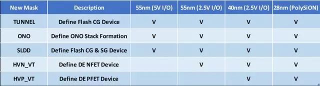
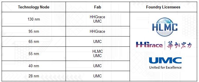
Available at 0.35µm, 0.13µm, 95nm, 65nm, 55nm, 40nm and 28nm process nodes.
-
Shipped>1,200,000 wafers from foundry partners HHGrace, HLMC and UMC.
-
Low cost, Lowpower, suitable for IoT, consumer, industrial, and automotive grade2/3 applications.
eCT : embedded Charge Trap
-
Former Spansion’s eNVM technology for automotive MCUs.
-
Based on 6 generations of Mirror Bit technologies.
-
In production (MCUs) at 40 nm node at UMC.
-
Automotive Grade-1 qualified.
Key Features
SONOS Introduction
Silicon Oxide Nitride Oxide Silicon
-
A planar, scalable MOS transistor with an ONO stack as the gate dielectric.
-
Store captured charges in discrete traps in the nitride (N) layer through FN tunneling.
Low Cost, Low Power, High Security
-
Lowest cost: Only 3~5 extra masks added into standard CMOS process.
-
Lowest power: 7.5V program/erase voltage, low-current FN/FN program/erase operations.
-
High Security: Resistant to decode by de-processing.
-
Ideal solution for consumer, industrial and especially IoT SoCs.
> MCU, Smart Card,EEPROM, FPGA, NOR Flash, etc.
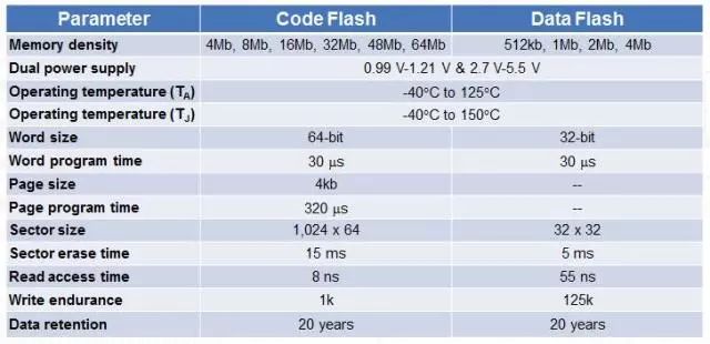
Key SONOS Macro Specs
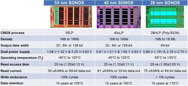
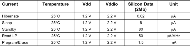
55 nm SONOS Macro Power Consumption
-
Balanced power consumption and performance (20ns Taa) for many applications
−Three power-saving modes: hibernate, sleep and standby.
−Low power read and program/erase operations to minimize active power.
−Low power read operation with Vdd=1.08 V to1.32 V.
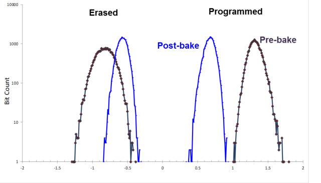
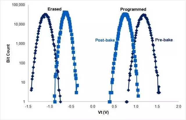
500hrs 225°C Yield w/ 50K Pre-cycling at 85 °C (55nm)
*All dies pass reading on full 8Mb after 500hrs 225°C bake
High Reliability
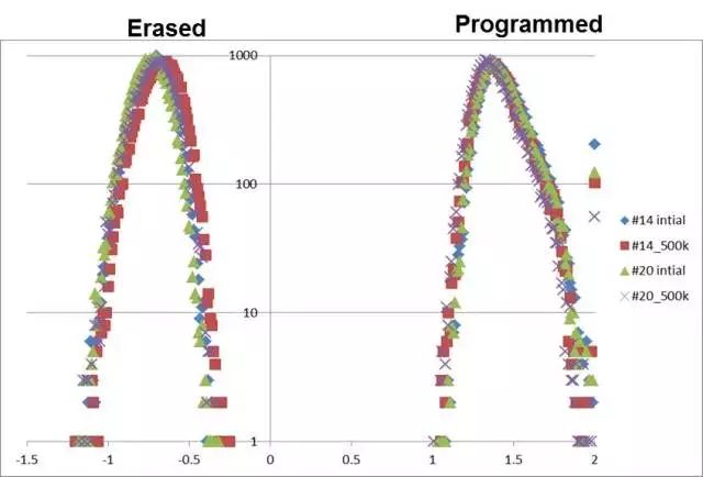
55-nm SONOS Macro Reliability
-
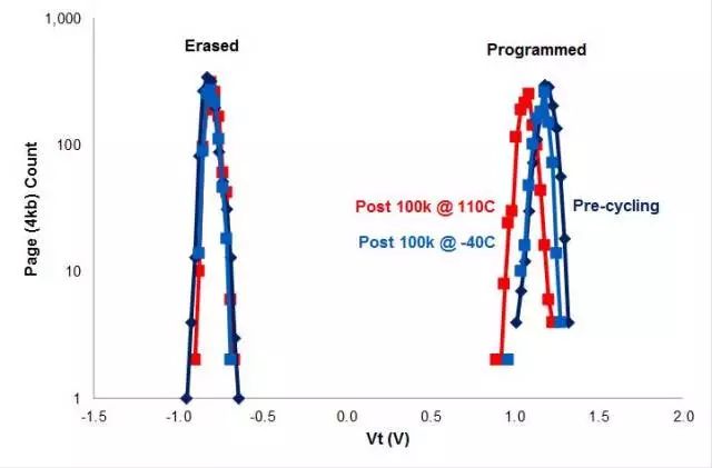
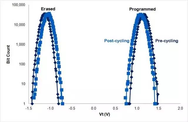
Endurance passes 500K cycles at 85°C w/o ECC. Vt window > 1.2V after 500K cycling.
-
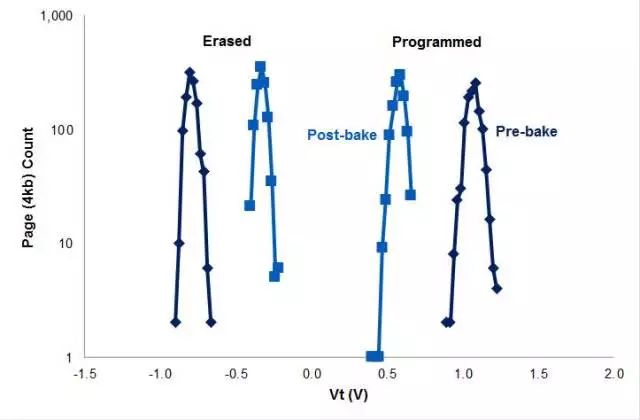
Retention passes Automotive Grade-2 AEC Q100 requirement.
> Vt window > 0.6 V after 500 hrs bake @ 225C with 50K pre-cycling.
>滑动查看下一张图片<
40-nm SONOS Macro Reliability
-
Endurance passes 500K cycles at 85°C w/o ECC. Vt window > 1.2V after 500K cycling.
-
Retention passes Automotive Grade-2 AEC Q100 requirement
>Vt window > 0.6 V after 500 hrs bake @ 225C with 50K pre-cycling.
>滑动查看下一张图片<
28-nm SONOS Macro Reliability
-
Endurance passes 10K cycles at 125°C, Vt window >1.4 V after cycling.
-
Retention passes accelerated 48-hour bake at 250°C with > 0.7 V window left.
>滑动查看下一张图片<
55nm SONOS in Production Press Release
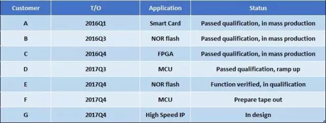
Customers NPI Status @ HLMC 55nm SONOS
-
Engaged > 15 customers.
-
7 Customers signed contract to use
-
3 in mass production
-
> 1,000 wafers started per month
SONOS eNVM Technology Availability
SONOS eNVM is scalable and proven in volume production on many nodes.
eCT Introduction
embedded Charge Trap
-
Based on charge-trap technology proven in six generations of MirrorBit® NOR Flash memory
Ideal solution for high-performance automotive MCUs
-
Fast 8 ns random access time from -40°C to 150°C junction temperature and 30 ms word programming speed
-
Smallest eNVM bit cell in the industry, 0.053 sq. µm, at 40 nm node
-
Automotive Grade-1 reliability
Applications
-
Hybrid and electric vehicle motor control, instrument clusters, body control modules and HVAC
-
In volume production on UMC 40LP process flow
Key eCT Macro Specs
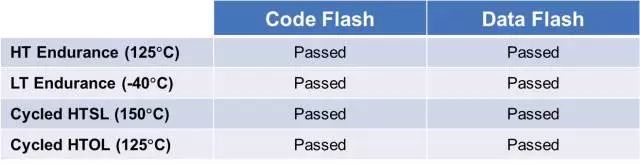
eCTReliability:
Automotive Qualification Data
-
Passed accelerated stress tests for Automotive Grade-1 per AEC-Q100 standard
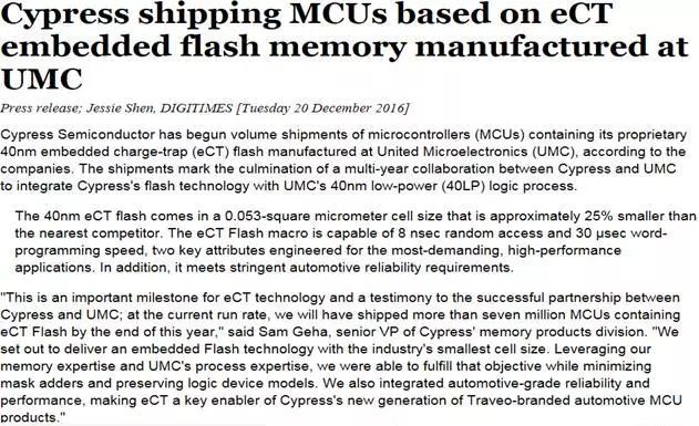
40nm eCT in Production Press Release
Embedded NVM Solutions for Various Applications
Conclusion
Cypress develops and licenses charge-trap NVM technologies and Flash macro IP
-
Charge-trap NVMs serve in a wide range ofembedded applications
−SONOS: Consumer, Industrial SoCs
−eCT: high-performance automotive MCUs,Automotive Grade-1 reliability
-
Technologies are scalable to advanced nodes
−SONOS in mass production from 0.35um to 55nm, engineering samples available on 40uLP & 28HLP
−eCT is in volume production on UMC 40LP process
-
Low power for IoT: 0.9 V (40nm) or 1.2V(55nm) power supply, low-current operation, power-saving modes
-
Cost-effective: 3~5 (SONOS) or 8 (eCT)extra masks beyond the standard CMOS.
-
[讨论]赛普拉斯芯片开发2010-02-10 0
-
赛普拉斯PSoC及其开发应用2012-11-19 0
-
赛普拉斯官方的PSoC® Creator培训教材2016-12-16 0
-
赛普拉斯900万像素CMOS图像传感器面向高端相机2018-10-24 0
-
赛普拉斯900万像素影像传感器2018-10-26 0
-
赛普拉斯CapSense方案一芯片可控制22个按键2018-11-02 0
-
BTC媒体中心键盘选用赛普拉斯激光导航传感器与无线HID解决方案2018-11-16 0
-
赛普拉斯手持终端用CMOS图像传感器方案2018-11-20 0
-
如何通过HTG-V6-PCIExpress板控制的赛普拉斯USB 2.0访问Virtex-6 FPGA2020-07-08 0
-
赛普拉斯IoT-AdvantEdge解决方案!2020-09-01 0
-
赛普拉斯存储器的解决方案!2020-09-01 0
-
【每日资料精选】赛普拉斯微控制器&解决方案资料合集!!!2020-09-01 0
-
赛普拉斯NV-SRAM解决方案分享2020-12-30 0
-
东莞回收赛普拉斯ic,高价收购赛普拉斯ic2021-09-27 0
全部0条评论

快来发表一下你的评论吧 !
