

NXP S32R274汽车雷达MCU开发方案解析
汽车电子
描述
nxp公司的S32R274是基于32位Power Architecture的用于汽车和工业雷达的MCU,安全核采用e200Z4 32位CPU,计算核采用e200Z7 32位CPU,集成了带ECC的2MB代码闪存(FMC闪存)和带ECC的1.5MB SRAM,雷达接口包括MIPI-CSI2 (4数据链),ΣΔ-ADC (4x 12位10 MSps)和DAC (10 MSps),其它接口包括Zipwire, 2x SAR-ADC, 2x SPI, 2x I2C, 3x FlexCAN (incl. 2x CAN-FD), Flexray™, LINFlexD和以太网,工作温度-40 到150˚ CAEC-Q100 Grade 1.本文介绍了S32R274主要特性,框图和系列产品性能比较表,以及评估板S32R274EVB主板和子板主要特性以及电路图.
The S32R27 is a 32-bit Power Architecture based microcontroller for automotive and industrial radar applications. It offers >4x leap in performance per power vs the previous MPC577X products, and increases the level of integration available to designers of next generation automotive radar modules. Designed to address advanced radar signal processing capabilities and merge it with microcontroller capabilities for generic software tasks and car bus interfacing. It meets the high performance computation demands required by modern beam-forming fast chirp modulation radar systems by offering unique signal processing acceleration together with powerful multi-core architecture.
S32R274主要特性:
• On-chip modules available within the device includethe following features:
• Safety core: Power Architecture? e200Z4 32-bit CPUwith checker core
• Dual issue computation cores: Power Architecture®e200Z7 32-bit CPU
• 2 MB on-chip code flash (FMC flash) with ECC
• 1.5 MB on-chip SRAM with ECC
• RADAR processing
– Signal Processing Toolbox (SPT) for RADAR signalprocessing acceleration
– Cross Timing Engine (CTE) for precise timinggeneration and triggering
– Waveform generation module (WGM) for chirpramp generation
– 4x 12-bit ΣΔ-ADC with 10 MSps
– One DAC with 10 MSps
– MIPICSI2 interface to connect external ADCs
• Memory Protection
– Each core memory protection unit provides 24entries
– Data and instruction bus system memory protectionunit (SMPU) with 16 region descriptors each
– Register protection
• Clock Generation
– 40 MHz external crystal (XOSC)
– 16 MHz Internal oscillator (IRCOSC)
– Dual system PLL with one frequency modulatedphase-locked loop (FMPLL)
– Low-jitter PLL to ΣΔ-ADC and DAC clockgeneration
• Functional Safety
– enables up to ASIL-D applications
– FCCU for fault collection and fault handling
– MEMU for memory error management
– Safe eDMA controller
– Self-Test Control Unit (STCU2)
– Error Injection Module (EIM)
– On-chip voltage monitoring
– Clock Monitor Unit (CMU)
• Security
– Cryptographic Security Engine (CSE2)
– Supports censorship and life-cycle management
• Timers
– Two Periodic Interval Timers (PIT) with 32-bitcounter resolution
– Three System Timer Module (STM)
– Three Software Watchdog Timers (SWT)
– Two eTimer modules with 6 channels each
– One FlexPWM module for 12 PWM signals
• Communication Interfaces
– Two Serial Peripheral interface (SPI) modules
– One LINFlexD module
– Two inter-IC communication interface (I2C)modules
– One dual-channel FlexRay module with 128message buffers
– Three FlexCAN modules with configurable buffers -CAN FD optionally supported on 2 FlexCANmodules
– One ENET MAC supporting MII/RMII/RGMIIinterface
– ZipWire high-speed serial communication
• Debug Functionality
– 4-pin JTAG interface and Nexus/Aurora interfacefor serial high-speed tracing
– e200Z7 core and e200Z4 core: Nexus developmentinterface (NDI) per IEEE-ISTO 5001-2012 Class 3+
• Two analog-to-digital converters (SAR ADC)
– Each ADC supports up to 16 input channels
– Cross Trigger Unit (CTU)
• On-chip voltage DC/DC regulator for core clock(VREG)
• Two Temperature Sensors (TSENS)
The following table provides a comparison of two devices S32R274 and MPC5775K .
This information is intended to provide an understanding of the range of functionality offered by this family. For full details of all of the family derivatives please contact your marketing representative.
S32R274系列产品比较表:
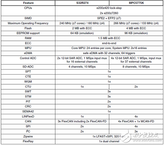
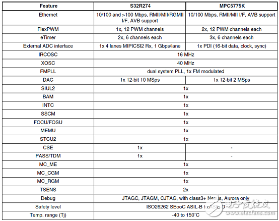
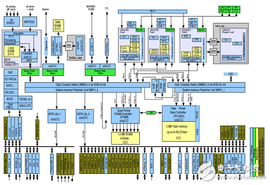
图1.S32R274框图
评估板S32R274EVB
The S32R274EVB evaluation board (EVB) is an evaluation tool for the S32R274 Radar MCU to enable hardware and software development.
For maximum flexibility and simplicity, the EVB has been designed as a modular development platform. The EVB main board does not contain an MCU. Instead, the MCU is fitted to an MCU daughter card (occasionally referred to as an adapter board). This approach means that the same EVB platform can be used for multiple packages and MCU derivatives within the MPC57xx and further families. High density connectors provide the interface between the EVB and MCU daughter cards as shown in the diagram below.
Both variants allow you to start with the software development, and to experience the highly integrated Radar Signal Processing Toolbox (SPT) along with state of the art functional safety and hardware security features (CSE2).
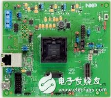
图2.评估板S32R274EVB外形图
评估板S32R274EVB包括不同特性的主板和子板.
主板主要特性:
• Support provided for different MCUs by utilising MCU daughter cards
• Single 12V external power supply input with four on-board regulators providing all of the necessary EVB and MCU voltages; Power supplied to the EVB via a 2.1mm barrel style power jack or a 2-way level connector; 12V operation allows in-car use if desired
• Master power switch and regulator status LEDs
• Two 240-way high-density daughter card expansion connectors allowing connection of the MCU daughter card or a custom board for additional application specific circuitry
• All MCU signals readily accessible at a port-ordered group of 0.1” pitch headers
• RS232/SCI physical interface and standard DB9 female connector
• FlexRAY interface
• LINFlexD interface
• 2 CAN interfaces, one configurable to be connected to one out of two CAN modules, and one connected to a dedicated third CAN module
• Ethernet interface
• Variable resistor, driving between 5V and ground
• 4 user switches and 4 user LEDs, freely connectable
• Liberal scattering of GND test points (surface mount loops) placed throughout the EVB
子板主要特性:
• MCU (soldered or through a socket)
• Flexible MCU clocking options allow provision of an external clock via SMA connector or 40MHz EVB clock oscillator circuit. Solder pads on the daughter card allow selection between these external clocks. SMA connectors (including differential clock input) on CLKIN signal for easy access.
• User reset switch with reset status LED
• Standard 14-pin JTAG debug connector and 34-pin Nexus Aurora connector
• 10-pin Serial Interprocessor Interface (SIPI) connector
• Gb Ethernet Physical interface IC, with RJ45 connector
• MIPI-CSI2 connector intended for use with Eagle MR3003 RADAR front end EVK (Evaluation Kit)
• Liberal scattering of ground and test points (surface mount loops) placed throughout the EVB
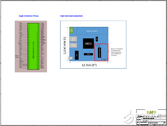
图3.评估板S32R274EVB电路图(1)
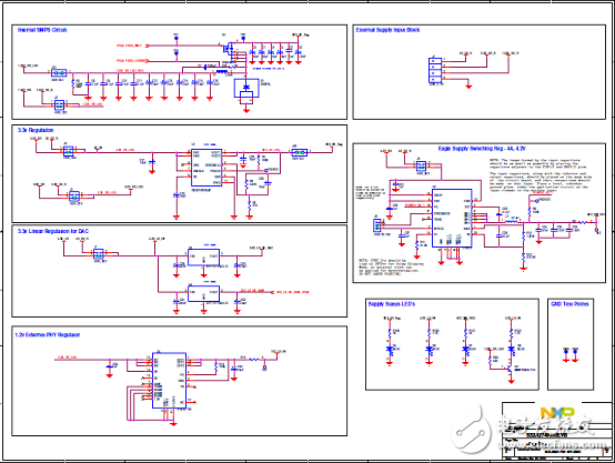
图4.评估板S32R274EVB电路图(2)
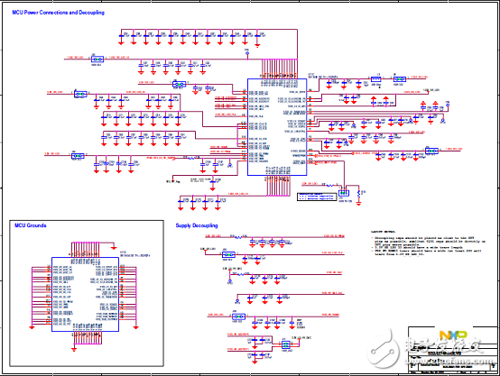
图5.评估板S32R274EVB电路图(3)
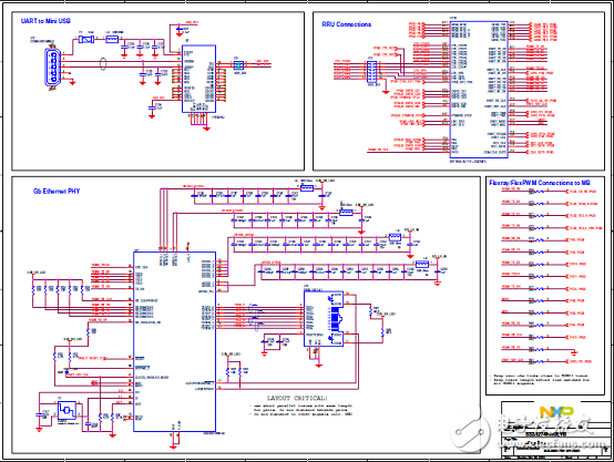
图6.评估板S32R274EVB电路图(4)
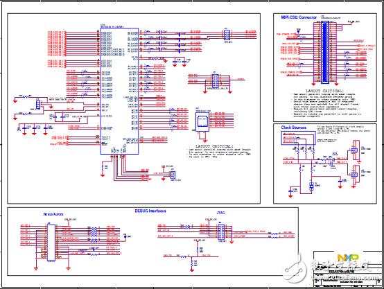
图7.评估板S32R274EVB电路图(5)
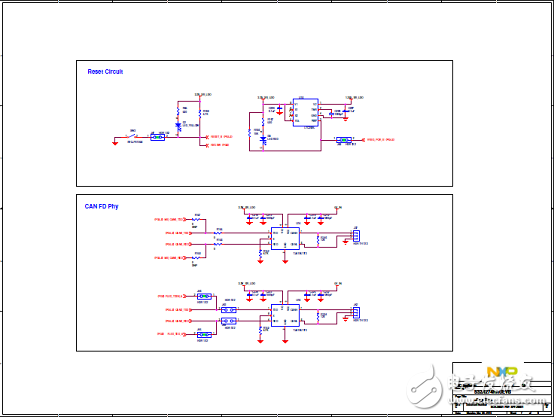
图8.评估板S32R274EVB电路图(6)
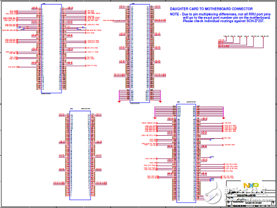
图9.评估板S32R274EVB电路图(7)
-
有没有S32R274的SPE功能详细的使用手册和例子可以参考呢2023-03-22 0
-
s32g274aevb启动时总是报错的原因?2023-05-06 0
-
Ameya360 汽车雷达系统解决方案2018-04-19 0
-
【看视频挖宝】NXP前沿技术抢先看,开发板、开发丛书、微信红包挖不停2018-11-21 0
-
汽车雷达传感器的解决方案2022-11-07 0
-
恩智浦加速量产S32R41高性能雷达处理器2023-03-14 0
-
NXP毫米波雷达开发工具2017-03-03 949
-
基于S32R274的汽车雷达MCU开发方案介绍2018-04-03 5534
-
贸泽电子供应NXP S32R274雷达微控制器2018-06-08 3284
-
贸泽电子即日起备货NXP Semiconductors的S32R274雷达微控制器2018-05-04 1137
-
关于NXP汽车安全解决方案的介绍(一)2018-06-28 4967
-
关于NXP汽车安全解决方案的介绍(二)2018-06-28 3287
-
02:基于S32R274的汽车雷达信号处理方案2019-01-24 3916
-
大联大世平集团推出基于NXP产品的先进辅助驾驶解决方案2019-11-07 1338
-
IAR Systems支持NXP S32K3 MCU系列下一代汽车应用2021-11-24 1614
全部0条评论

快来发表一下你的评论吧 !
