

ADI 四路高性能低噪声降压调节器--ADP5014特性详解
电源/新能源
描述
ADI公司的ADP5014是在6 mm × 6 mm 40引脚LFCSP封装中集成四路高性能低噪声降压调节器,其所有通道均集成高端和低端功率金属氧化物半导体场效应晶体管(MOSFET).通道1和通道2同时提供2 A或4 A的可编程输出电流,通道3和通道4同时提供1 A和2 A的可编程输出电流.其它特性包括可选强制脉冲宽度调制(FPWM)/省电模式(PSM),欠压输出(UVO),有源输出放电和电源良好指示.安全特性包括输入欠压闭锁(UVLO),过压保护(OVP),过流保护(OCP)和热关断(TSD).输入电压2.75V-6.0V,可编输出电压0.5V-0.9xVINx.主要用在RF收发器,高速模数转换器(ADC)/数模转换器(DAC),混合信号ASIC,现场可编程门阵列(FPGA)和处理器应用,安防和监控以及医疗应用.本文介绍了ADP5014主要特性,功能框图,典型应用电路,以及评估板ADP5014-EVALZ主要特性,电路图,材料清单和PCB设计图.
The ADP5014 combines four high performance, low noise buckregulators in a 40-lead LFCSP package. Relying on its lowoutput noise (~25 μVrms when VOUT ≤ VREF), the low noisebuck regulator enables the powering up of the noise sensitivesignal chain products.
All channels in the ADP5014 integrate high-side and low-sidepower metal-oxide semiconductor field effect transistors(MOSFET). Channel 1 and Channel 2 deliver a programmableoutput current of 2 A or 4 A. Combining Channel 1 andChannel 2 in a parallel configuration provides a single outputwith up to 8 A of current.
Channel 3 and Channel 4 deliver a programmable output currentof 1 A or 2 A. Combining Channel 3 and Channel 4 in a parallelconfiguration can provide a single output with up to 4 A of current.
The ADP5014 features two enable modes. The manual modehas four individual precision enable pins to enable eachregulator manually. Alternatively, the sequence mode has one grouped precision enable signal with programmable power-upand power-down delay timers on each rail for specific railsequence requirements.
The switching frequency of the ADP5014 can be programmedor synchronized to an external clock from 500 kHz to 2.5 MHz.The ADP5014 offers other key features like selective forcedpulse width modulation (FPWM)/power saving mode (PSM),an undervoltage output (UVO), active output discharge, and apower-good flag. Other safety features include input undervoltagelockout (UVLO), overvoltage protection (OVP),overcurrent protection (OCP) and thermal shutdown (TSD).
ADP5014主要特性:
Input voltage range: 2.75 V to 6.0 V
Programmable output voltage range: 0.5 V to 0.9 × PVINx
Low output noise: ~25 μVrms when VOUT ≤ VREF±1.0% output accuracy over full temperature range500 kHz to 2.5 MHz adjustable switching frequency
Power regulation
Channel 1 and Channel 2: programmable 2 A/4 A syncbuck regulators, or single 8 A output in parallel
Channel 3 and Channel 4: programmable 1 A/2 A syncbuck regulators, or single 4 A output in parallel
Flexible parallel operation
Precision enable with 0.6 V threshold
Manual or sequence mode for power-up and power-downsequence
Selective FPWM or PSM operation mode
Precision undervoltage comparator
Frequency synchronization input or output
Active output discharge switch
Power-good flag on selective channels via factory fuse
UVLO, OVP, OCP, and TSD protection
40-lead, 6 mm × 6 mm LFCSP package
−40 ℃ to +125 ℃ junction temperature
ADP5014应用:
RF transceiver, high speed analog-to-digital converter
(ADC)/digital-to-analog converter (DAC), mixed signal ASIC
FPGA and processor applications
Security and surveillance
Medical applications
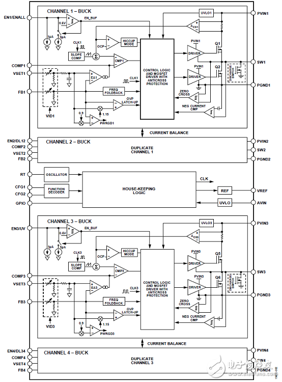
图1. ADP5014功能框图
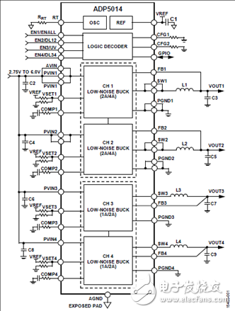
图2. ADP5014典型应用电路图(1)
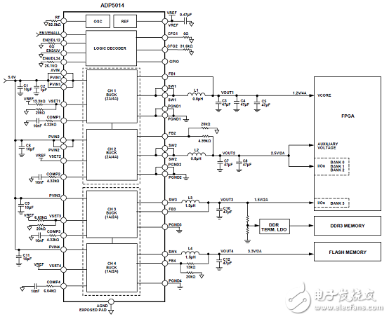
图3. ADP5014典型应用电路图(2):FPGA应用,1.2MHz开关频率,顺序使能模式
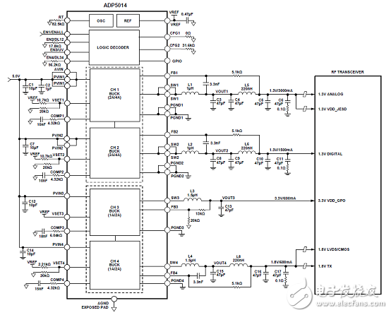
图4. ADP5014典型应用电路图(2):RF收发器应用,1.2MHz开关频率,顺序使能模式
评估板ADP5014-EVALZ
This user guide describes the evaluation of the ADP5014 and includes detailed schematics and printed circuit board (PCB) layouts.
The ADP5014-EVALZ evaluation board combines four high performance buck regulators in a 40-lead LFCSP package to meet the demanding performance and board space requirements.
Full details on the ADP5014 regulator are provided in the ADP5014 data sheet, available from Analog Devices, Inc. Consult the data sheet in conjunction with this user guide when working with this evaluation board.
评估板ADP5014-EVALZ主要特性:
Full featured evaluation board for the ADP5014
Compact solution size
4-layer high glass transition temperature (TG) PCB for superior thermal performance
Convenient connections through vertical printed circuit tail pin headers
Supply voltage
2.75 V to 6.0 V for PVINx
Mode option to select manual or sequence enable
Mode option to select PSM or FPWM operation
Programmable switching frequency from 500 kHz to 2.5 MHz
Frequency synchronization input or output
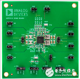
图5.评估板ADP5014-EVALZ外形图
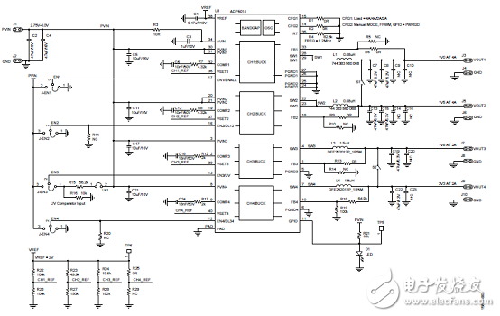
图6.评估板ADP5014-EVALZ电路图
评估板ADP5014-EVALZ材料清单(BOM):
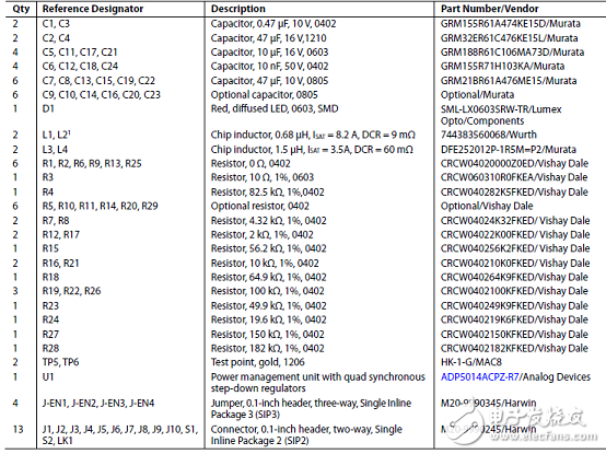
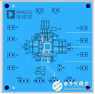
图7.评估板ADP5014-EVALZ PCB设计图(1)
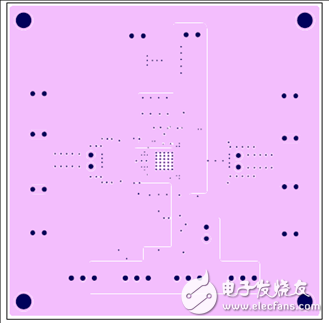
图8.评估板ADP5014-EVALZ PCB设计图(2)
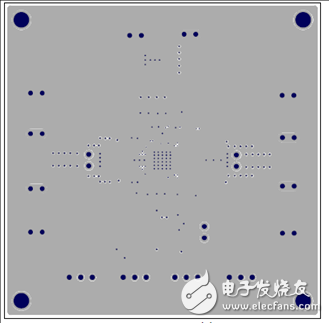
图9.评估板ADP5014-EVALZ PCB设计图(3)
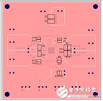
图10.评估板ADP5014-EVALZ PCB设计图(4)
详情请见:
和
ADP5014-EVALZ-UG-1137.pdf
-
在系统中成功运用DC-DC降压/升压调节器2018-11-01 0
-
ADP2323/25双通道降压DC-DC调节器的性能特点及应用2019-07-08 3400
-
ADP2118同步降压型调节器的性能分析2019-06-12 2644
-
ADP5014 Buck Design Tool2021-02-05 405
-
ADP150:超低噪声、150mA CMOS线性调节器2021-03-18 480
-
ADP151:超低噪声、200 mA CMOS线性调节器2021-03-18 480
-
ADP222/ADP223/ADP224/ADP225:双通道、300 mA输出、低噪声、高PSRR电压调节器2021-03-20 434
-
ADP320:三倍、200 mA、低噪声、高电源抑制比电压调节器2021-04-17 470
-
ADP322/ADP323:三倍、200 mA、低噪声、高电源抑制比电压调节器数据表2021-04-17 455
-
ADP220/ADP221:双通道、200 mA、低噪声、高电源抑制比电压调节器数据表2021-04-26 555
-
ADP1765:5 A,低VIN,低噪声,CMOS线性调节器数据表2021-05-07 455
-
ADP5014:采用四路低噪声降压稳压器的集成电源解决方案数据表2021-05-14 462
-
UG-1137:评估ADP5014 4通道电源管理单元2021-05-26 493
-
ADP5014降压设计工具2021-06-02 494
全部0条评论

快来发表一下你的评论吧 !
