

基于FPU的超低功耗高性能ARM MCU穿戴应用开发方案
电子说
描述
Maxim公司的MAX32625/MAX32626是基于FPU的超低功耗高性能ARM® Cortex®-M4 MCU.该架构包括了超低功耗高效率信号处理功能和容易使用,内部96MHz振荡器提供了高性能,而4MHz振荡器支持需要常开监视功能的最低功耗。器件集成了512KB闪存和160KB SRAM,核电压1.2V,I/O电压1.8V-3.3V,主要用在运动手表,健身监理器,可穿戴医疗贴件,手持医疗设备和传感器集线器。本文介绍了MAX32625/MAX32626主要优势和特性,框图,典型应用电路图以及评估板MAX32625/MAX32626EVK主要优势和特性,框图和电路图。
The MAX32625/MAX32626 are ARM® Cortex®-M4 with FPU-based microcontrollers, ideal for the emerging category of wearable medical and fitness applications. The architecture combines ultra-low power, high-efficiency signal processing functionality and ease of use. An internal 96MHz oscillator provides high-performance capability, and the internal 4MHz oscillator supports minimal power consumption for applications requiring always-on monitoring. The device provides 512kB of flash and 160kB of SRAM.
The device features four powerful and flexible power modes. A peripheral management unit (PMU) enables intelligent peripheral control with up to six channels to significantly reduce power consumption. Built-in dynamic clock gating and firmware-controlled power gating allows the user to optimize power for the specific application.
Multiple SPI, UART, and I2C serial interfaces are provided, as well as a 1-Wire® master and USB, allowing for interconnection to a wide variety of external sensors. A four-input, 10-bit delta-sigma ADC monitors analog input from external sensors. The MAX32625L is a lower-cost version of the MAX32625, providing 256kB of flash and 128kB of SRAM.
The MAX32626 is a secure version of the MAX32625. It incorporates a trust protection unit (TPU) with encryption and advanced security features. These features include a modular arithmetic accelerator (MAA) for ECDSA, a hardware TRNG entropy generator, and a secure boot loader. Both the MAX32626 and the MAX32625 provide a hardware AES engine.
MAX32625/MAX32626主要优势和特性:
High-Efficiency Microcontroller for Wearable DevicesInternal Oscillator Operates Up to 96MHz
Low Power 4MHz Oscillator System Clock Option for Always-On Monitoring Applications
512KB Flash Memory (256KB “L” Version)
160KB SRAM (128KB“L”Version)
8KB Instruction Cache
1.2V Core Supply Voltage
1.8V to 3.3V I/O
Optional 3.3V ±5% USB Supply Voltage
Wide Operating Temperature: -30℃ to +85℃
Power Management Maximizes Uptime for Battery Applications106μA/MHz Active Current Executing from Cache
49μA/MHz Active Current Executing from Flash
Wake-Up to 96MHz Clock or 4MHz Clock
600nA Low Power Mode (LP0) Current with RTC Enabled
2.56μW Ultra-Low Power Data Retention Sleep Mode (LP1) with Fast 5μs Wake-Up on 96MHz Clock Source
27μA/MHz Low Power Mode (LP2) Current
Optimal Peripheral Mix Provides Platform ScalabilitySPI Execute in Place (SPIX) Engine for Memory Expansion with Minimal Footprint
Three SPI Masters, One SPI Slave
Three UARTs
Up to Two I2C Masters, One I2C Slave
1-Wire Master
Full-Speed USB 2.0 Device with Internal Transceiver
Sixteen Pulse Train (PWM) Engines
Six 32-Bit Timers and 3 Watchdog Timers
Up to 40 General-Purpose I/O Pins
10-Bit Delta-Sigma ADC Operating at 7.8ksps
AES -128, -192, -256
CMOS-Level 32kHz RTC Output Available in All Power Modes
Secure Valuable IP and Data with Robust Internal Hardware Security (MAX32626 Only)Trust Protection Unit (TPU) Provides ECDSA and Modular Arithmetic Acceleration Support
True Random Number Generator
Secure Boot Loader
MAX32625/MAX32626应用:
Sports Watches
Fitness Monitors
Wearable Medical Patches
Portable Medical Devices
Sensor Hubs
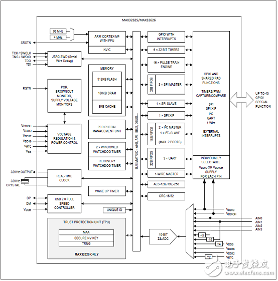
图1.MAX32625/MAX32626框图
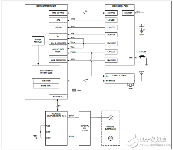
图2. MAX32625/MAX32626典型应用电路图
评估板MAX32625/MAX32626EVK
The MAX32625/MAX32626 evaluation kit (EV kit) provides a convenient platform for evaluating the capabilities of the MAX32625/MAX32626 microcontroller. The EV kit also provides a complete, functional system ideal for developing and debugging applications.
评估板MAX32625/MAX32626EVK主要优势和特性:
Easily Load and Debug Code Using the Supplied Olimex ARM-USB-TINY-H JTAG Debugger Connected Through a Standard 20-Pin ARM JTAG Header
Selectable Power Sources for PMIC Include USB Power Through the CN1 or CN2 Connector, Optional External Battery Through J2 Connector, or Bench Supply Through Test Points TP8 and TP9
Selectable Power Source for On-Board Peripherals (Switches, LEDs, OLED Display, SPI Flash, Bluetooth® LE Transceiver)
Headers for Accessing the IC ’s I/O Pins and Analog Front End (AFE) Input Signals
USB Micro-B Connection to the IC’s USB Device Controller
USB Micro-B Connection to USB-UART Bridge Selectable Between the IC’s Internal UART 0 and UART 1
On-Board Bluetooth 4.0 BLE Transceiver with Chip Antenna
General-Purpose Pushbutton Switches and Indicator LEDs (All Connected to GPIOs) for User I/O
Prototyping Matrix (0.1in Grid) with Integrated Power Rails for Customer Circuitry
评估板MAX32625/MAX32626EVK包括:
EV kit board with a MAX32625 or MAX32626 microcontroller
Olimex ARM-USB-TINY-H JTAG debugger with JTAG ribbon cable (for connecting from debugger to EV kit header J1) and USB standard A-to-B cable (for connecting from PC to debugger)
Standard-A to Micro-B USB cable (for connecting from PC or standalone USB power supply to EV kit USB Micro-B connector CN2) allows connection from PC USB host to the IC’s USB device controller peripheral
Standard-A to Micro-B USB cable (for connecting PC to EV kit USB connector CN1) allows virtual COM port interface to the IC’s UART 0 or UART 1 through a USB/UART bridge
MAX32625/MAX32626 EV Kit Quick Start Guide
Hex Keys for the Socket (MAX32626 EV Kit Only)
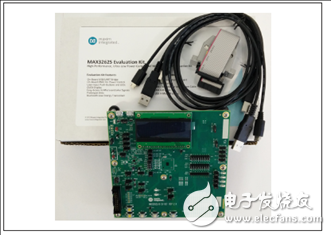
图3.评估板MAX32625EVK套件外形图
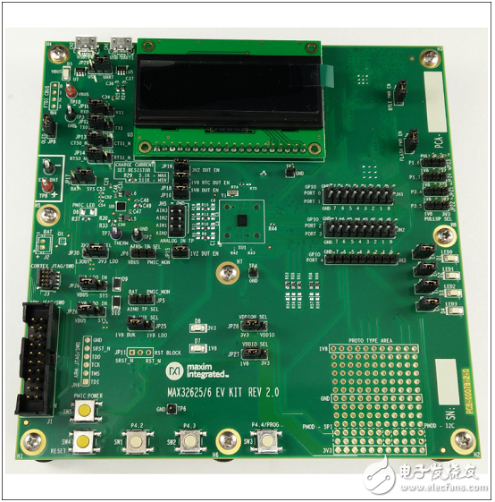
图4.评估板MAX32625/6EVK外形图
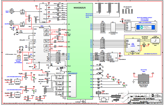
图5.评估板MAX32625/6EVK框图
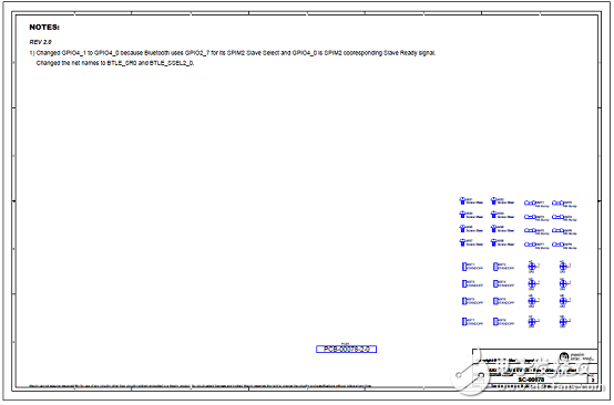
图6.评估板MAX32625/6EVK电路图(1)
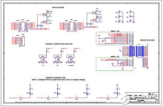
图7.评估板MAX32625/6EVK电路图(2)
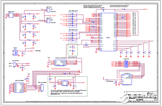
图8.评估板MAX32625/6EVK电路图(3)
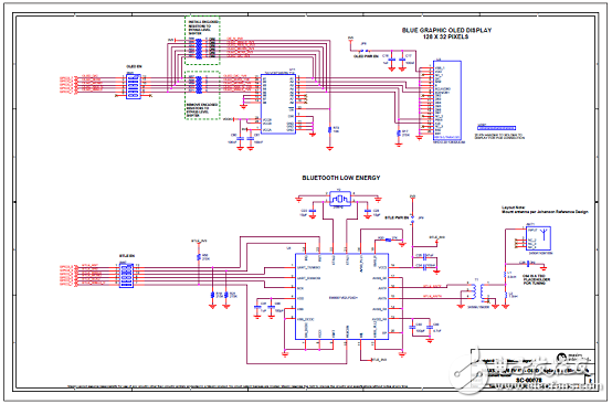
图9.评估板MAX32625/6EVK电路图(4)
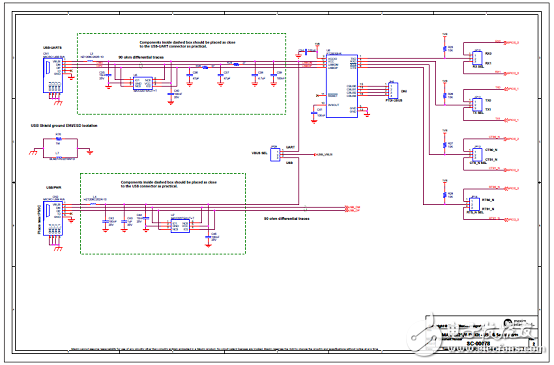
图10.评估板MAX32625/6EVK电路图(5)
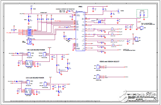
图11.评估板MAX32625/6EVK电路图(6)
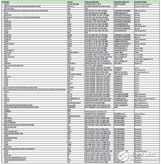
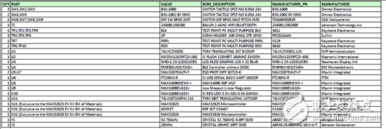
评估板MAX32625/6EVK材料清单:
-
小尺寸、超低功耗的智能穿戴定位解决方案2017-09-28 0
-
全新的超低功耗MSP432 MCU2018-08-07 0
-
ARM超低功耗实体IP对MCU发展有什么影响2019-07-22 0
-
超低功耗MCU在物联网方案中的应用2023-06-13 0
-
基于STM8L15xxx设计的超低功耗8位MCU开发方案2010-05-17 4130
-
ST STM32L4R9I高性能超低功耗ARM MCU开发方案2017-11-30 2391
-
ST发布匠心巨作STM32L4+_低功耗高性能你值得拥有2018-05-12 20896
-
ARM M4F联手CMOS,共同开发穿戴可产品中的超低功耗心率监测解决方案2018-06-25 1876
-
MAX32631用于可穿戴设备的具有FPU的ARM MCU2019-05-01 924
-
藍牙4.0 超低功耗藍牙空中鼠標解決方案2018-10-04 275
-
STM32L496xx系列超低功耗32位ARM MCU开发方案2019-05-01 8530
-
PSoC 6高性能超低功耗IoT应用方案2019-05-11 4004
-
RM0434 基于 Arm® 的 Cortex®-M4多协议无线 32 位 MCU ,带有 FPU、Bluetooth® 低功耗和 802.15.4 无线电解决方案2022-11-23 252
-
DS13737 超低功耗Arm® Cortex®-M33 32位MCU+TrustZone®+FPU,240 DMIPS,2MB闪存,786 KB SRAM2022-11-23 260
-
DS11584 STM32L4A6xG 超低功耗 Arm® Cortex®-M4 32 位 MCU+FPU数据手册2022-11-23 231
全部0条评论

快来发表一下你的评论吧 !
