

Intel MAX 10 FPGA系列低成本开发方案大合集
FPGA/ASIC技术
描述
Intel公司的MAX 10 FPGA系列采用TSMC 55nm NOR闪存技术,容量从2K到50K 逻辑单元(LE),采用单个或双核电源电压和小尺寸3x3mm和高I/O引脚数封装;器件具有全特性FPGA功能,支持Nios II软核嵌入处理器,数字信号处理(DSP)区块以及软DDR3存储器控制器,内部存储双配置闪存,用户闪存存储器,集成了模数转换器(ADC).主要用在系统管理,I/O扩展,通信控制,工业应用,汽车电子和消费类电子.本文介绍了Intel® MAX® 10 FPGA系列主要优势,器件平面布局图以及MAX 10 FPGA开发套件主要特性和电路图.
Intel® MAX® 10 FPGAs revolutionize non-volatile integration by delivering advanced processing capabilities in a low-cost, single chip small form factor programmable logic device. Building upon the single chip heritage of previous MAX device families, densities range from 2K – 50K LEs, using either single or dual-core voltage supplies. The MAX 10 FPGA family encompasses both advanced small wafer scale packaging (3 mm x 3 mm) and high I/O pin count packages offerings.
MAX 10 FPGAs are built on TSMC’s 55 nm embedded NOR flash technology, enabling instant-on functionality. Integrated features include analog-to-digital converters (ADCs) and dual configuration flash allowing you to store and dynamically switch between two images on a single chip. Unlike CPLDs, MAX 10 FPGAs also include full-featured FPGA capabilities, such as Nios® II soft core embedded processor support, digital signal processing (DSP) blocks, and soft DDR3 memory controllers.
Intel® MAX® 10 devices are single-chip, non-volatile low-cost programmable logic devices (PLDs) to integrate the optimal set of system components.
The highlights of the Intel MAX 10 devices include:
• Internally stored dual configuration flash
• User flash memory
• Instant on support
• Integrated analog-to-digital converters (ADCs)
• Single-chip Nios II soft core processor support
The MAX? 10 devices consist of the following:
• Logic array blocks (LABs)
• Analog-to-digital converter (ADC)
• User flash memory (UFM)
• Embedded multiplier blocks
• Embedded memory blocks (M9K)
• Clocks and phase-locked loops (PLL)
• General purpose I/O
• High-speed LVDS I/O
• External memory interfaces
• Configuration flash memory (CFM)
Intel MAX 10 devices are the ideal solution for system management, I/O expansion,
communication control planes, industrial, automotive, and consumer applications.
Intel® MAX® 10 FPGA系列主要优势:
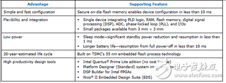
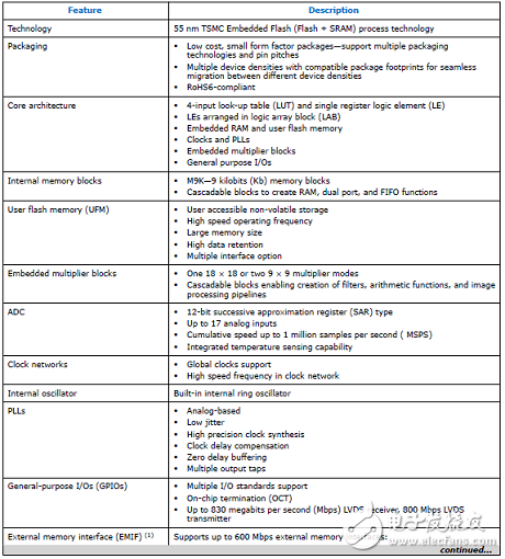
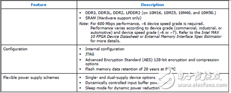
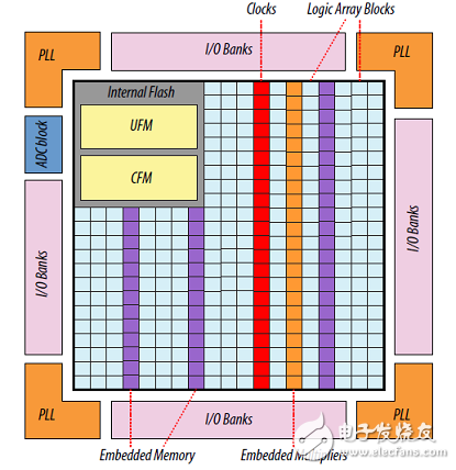
图1. Intel® MAX® 10 FPGA器件平面布局图
MAX 10 FPGA开发套件
The MAX? 10 FPGA development board provides a hardware platform for evaluating the performanceand features of the Altera? MAX 10 device.
The development kit includes a RoHS- and CE-compliant MAX 10 FPGA Development board with thefollowing components:
• Featured Devices:
• MAX 10 FPGA (10M50D, dual supply, F484 package)
• Enpirion? EN2342QI 4 A PowerSoC Voltage-Mode Synchronous Step-Down Converter withIntegrated Inductor Enpirion
• EN6337QI 3 A High-Efficiency PowerSoC DC-DC Step-Down Converters with Integrated Inductor
• Enpirion EP5358xUI 600 mA PowerSoC DC-DC Step-Down Converters with Integrated Inductor
• MAX II CPLD – EPM1270M256C4N (On-board USB-Blaster™ II)
• Programming and Configuration:
• Embedded USB-Blaster II (JTAG)
• Optional JTAG direct via 10-pin header
• Memory Devices:
• 64-Mx16 1 Gb DDR3 SDRAM with soft memory controller
• 128-Mx8 1 Gb DDR3 SDRAM with soft memory controller
• 512-Mb Quad serial peripheral interface (quad SPI) flash
• Communication Ports:
• Two Gigabit Ethernet (GbE) RJ-45 ports
• Ethernet Port A (Bottom)
• Ethernet Port B (Top)
• One mini-USB2.0 UART
• One high-definition multimedia interface (HDMI) video output
• One universal high-speed mezzanine card (HSMC) connector
• Two 12-pin DigilentPmod™ compatible connectors
• Analog:
• Two MAX 10 FPGA analog-to-digital converter (ADC) SMA inputs
• 2x10 ADC header
• Potentiometer input to ADC
• One external 16 bit digital-to-analog converter (DAC) device with SMA output
• Clocking
• 25 MHz single-ended, external oscillator clock source
• Silicon labs clock generator with programmable frequency GUI
• Mini-USB cable for on-board USB-Blaster™ II
• 2A Power Supply and cord
• Free Quartus? II Web Edition design software (download software and license from website)
• Complete documentation
• User manual, bill of materials, schematic, and board files
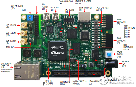
图2. MAX 10 FPGA开发板正面元件图
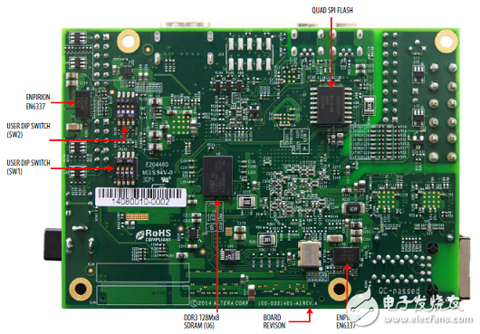
图3. MAX 10 FPGA开发板背面元件图
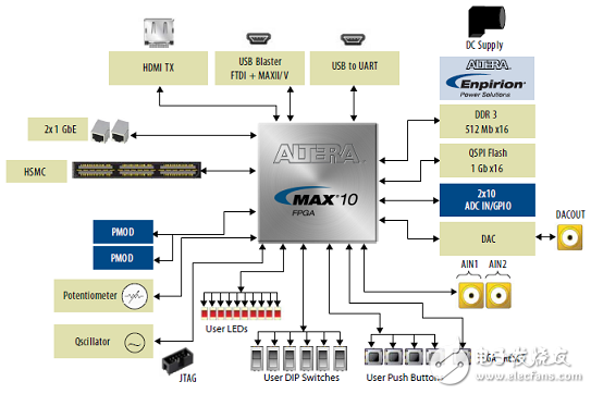
图4. MAX 10 FPGA开发板系统框图
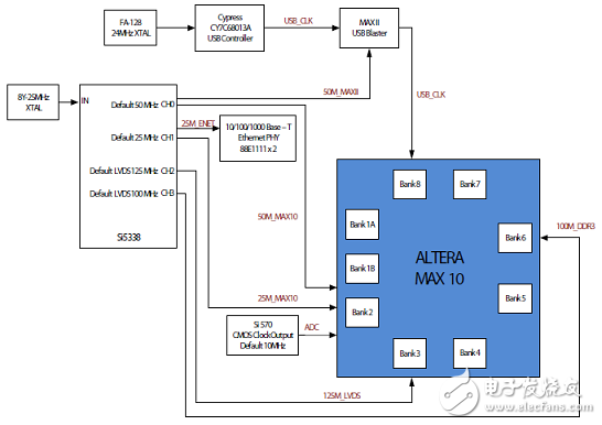
图5. MAX 10 FPGA开发板时钟框图
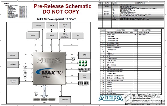
图6. MAX 10 FPGA开发板电路图(1)
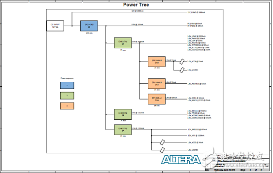
图7. MAX 10 FPGA开发板电路图(2)
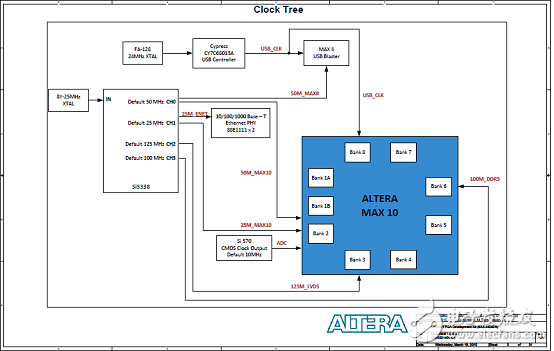
图8. MAX 10 FPGA开发板电路图(3)
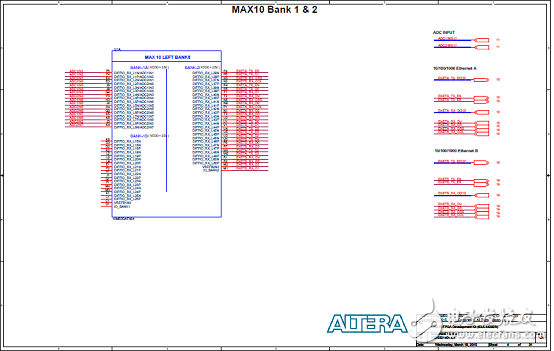
图9. MAX 10 FPGA开发板电路图(4)
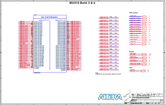
图10. MAX 10 FPGA开发板电路图(5)
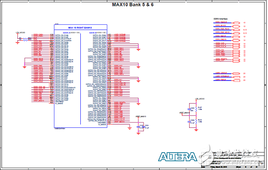
图11. MAX 10 FPGA开发板电路图(6)
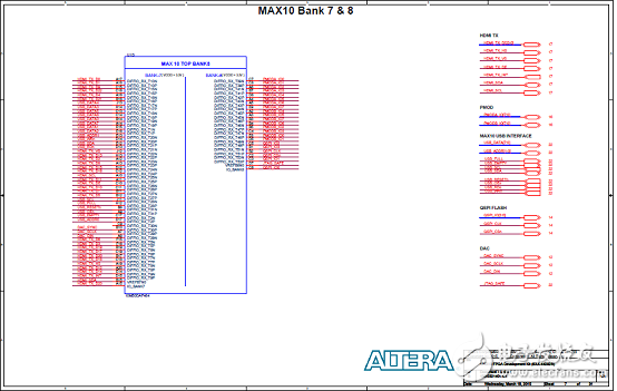
图12. MAX 10 FPGA开发板电路图(7)
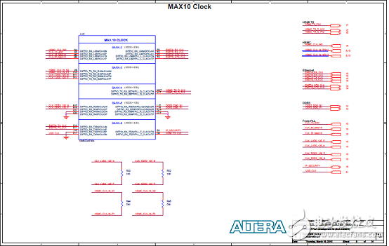
图13. MAX 10 FPGA开发板电路图(8)

图14. MAX 10 FPGA开发板电路图(9)
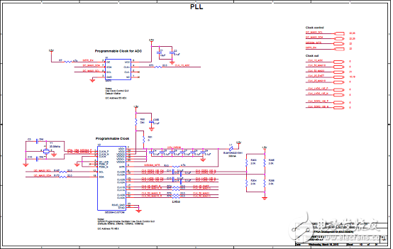
图15. MAX 10 FPGA开发板电路图(10)
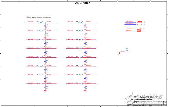
图16. MAX 10 FPGA开发板电路图(11)
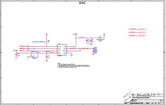
图17. MAX 10 FPGA开发板电路图(12)
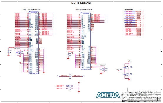
图18. MAX 10 FPGA开发板电路图(13)
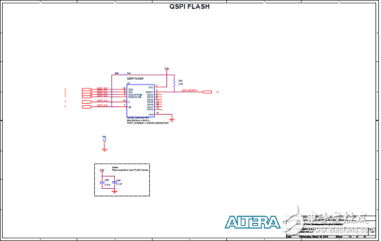
图19. MAX 10 FPGA开发板电路图(14)
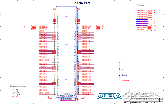
图20. MAX 10 FPGA开发板电路图(15)
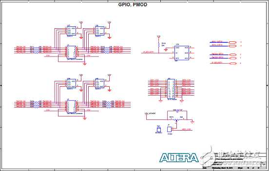
图21. MAX 10 FPGA开发板电路图(16)
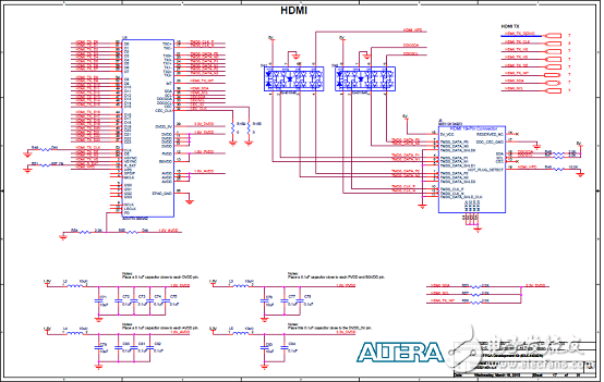
图22. MAX 10 FPGA开发板电路图(17)
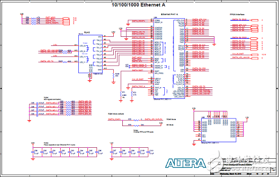
图23. MAX 10 FPGA开发板电路图(18)
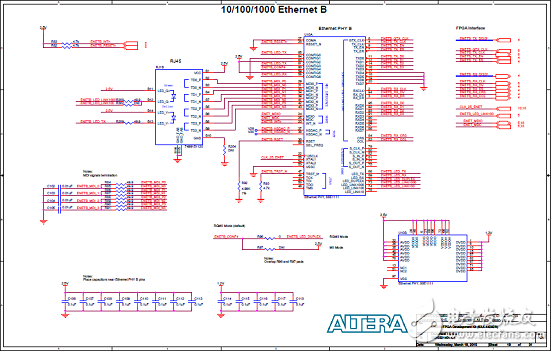
图24. MAX 10 FPGA开发板电路图(19)
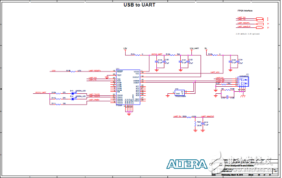
图25. MAX 10 FPGA开发板电路图(20)
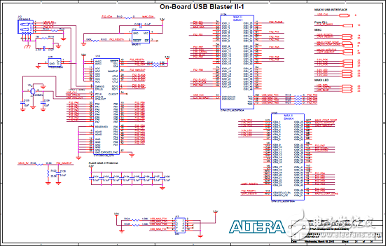
图26. MAX 10 FPGA开发板电路图(21)
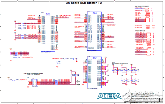
图27. MAX 10 FPGA开发板电路图(22)
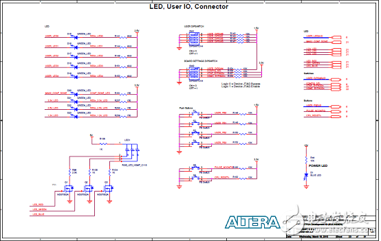
图28. MAX 10 FPGA开发板电路图(23)
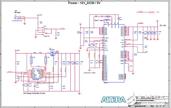
图29. MAX 10 FPGA开发板电路图(24)
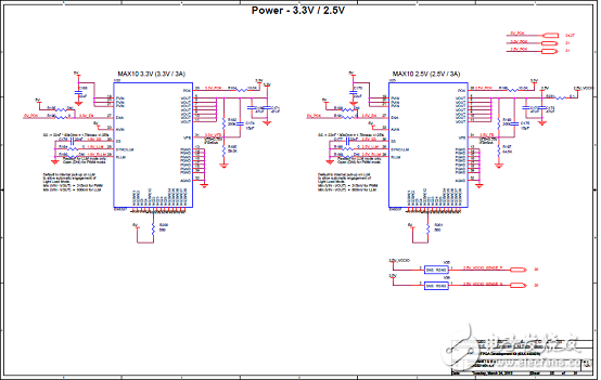
图30. MAX 10 FPGA开发板电路图(25)
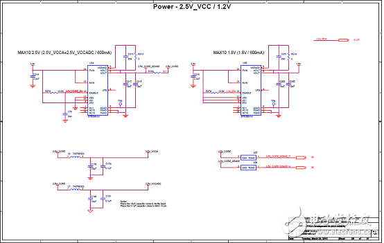
图31. MAX 10 FPGA开发板电路图(26)
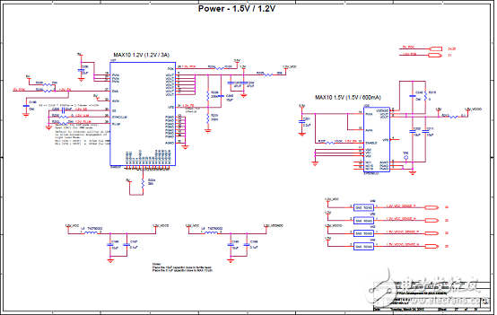
图32. MAX 10 FPGA开发板电路图(27)
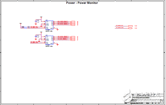
图33. MAX 10 FPGA开发板电路图(28)
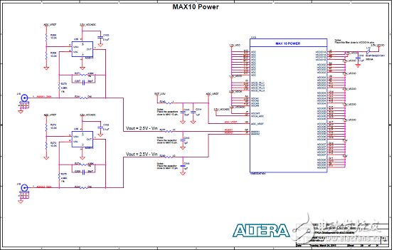
图34. MAX 10 FPGA开发板电路图(29)
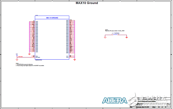
图35. MAX 10 FPGA开发板电路图(30)
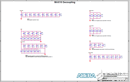
图36. MAX 10 FPGA开发板电路图(31)
-
低成本蓝牙串口模块解决方案2014-03-21 0
-
Intel Max10 FPGA命名规范电子学习 2022-12-09
-
Intel Max10 FPGA主要应用电子学习 2022-12-09
-
4-20mA一路转多路信号隔离放大低成本、小体积解决方案2010-02-22 0
-
MAX 10 FPGA的特性2019-07-01 0
-
什么是Altera系列低成本Cyclone IV FPGA?2019-07-31 0
-
使用STM32F10xxx实现低成本现实的应用方案2022-12-01 0
-
基于MAX17014的低成本LCD TV电源解决方案2010-03-24 833
-
LatticeECP4系列:低成本、低功耗FPGA2012-06-06 1954
-
Altera起价只有49美元的开发套件扩展了低成本系列产品2013-10-15 1153
-
Step-by-step-design-of-a-basic-embedded-system-using-an-Intel-MAX10-FPGA.pdf2017-01-22 916
-
一种基于低成本FPGA的高速8B_10B编解码器设计_陈章进2017-03-19 683
-
高效、低成本的 FPGA 器件:Spartan-7 FPGA!2017-11-16 8460
-
Altera发布MAX 10:业界首款多功能、低成本单芯片FPGA2018-10-28 3922
-
贸泽开售用于PCIe 4.0 设计的Intel Agilex F系列FPGA开发套件2021-02-04 2497
全部0条评论

快来发表一下你的评论吧 !
