

DLP4500主要特性 DLP 3D打印机特性
工业控制
描述
TI公司的DLP4500数字微镜器件 (DMD)是一款数控 MOEMS(微光机电系统)空间照明调制器(SLM),可锁存,电进/光出半导体器件。DLP4500可生成具有速度,精度和效率的光发射图样,非常适合于使用结构光的3D扫描或度量,扩增实境,显微镜,医疗仪器和光谱分析等应用。本文介绍了DLP4500主要特性,框图和典型系统框图以及其DLP 3D打印机主要特性,框图,电路图和材料清单.
The DLP4500 digital micromirror device (DMD) is a digitally controlled MOEMS (micro-opto-electromechanical system) spatial light modulator (SLM). When coupled to an appropriate optical system, the DLP4500 can be used to modulate the amplitude and/or direction of incoming light. The DLP4500 creates light patterns with speed, precision, and efficiency.
Architecturally, the DLP4500 is a latchable, electrical-in/optical-out semiconductor device. This architecture makes the DLP4500 well suited for use in applications such as 3D scanning or metrology with structured light, augmented reality, microscopy, medical instruments, and spectroscopy. The compact physical size of the DLP4500 is well-suited for portable equipment where small form factor and lower cost are important. The compact package compliments the small size of LEDs to enable highly efficient, robust light engines.
The DLP4500 is one of two devices in the DLP 0.45 WXGA chip set (see ). Proper function and reliable operation of the DLP4500 requires that it be used in conjunction with the DLPC350 controller. See the DLP 0.45 WXGA Chip-set data sheet (TI literature number DLPU009) for further details. shows a typical system application using the DLP 0.45-inch WXGA chip set.
DLP4500主要特性:
0.45-Inch (11.43 mm) Diagonal Micromirror Array
912 × 1140 Array of Aluminum, Micrometer-Sized Mirrors
7.6-µm Micromirror Pitch
±12° Micromirror Tilt Angle (Relative to Flat State)
Side Illumination for Optimized Efficiency
3-µs Micromirror Cross Over Time
Highly Efficient in Visible Light (420 nm–700 nm):
Window Transmission 97% (Single Pass, Through Two Window Surfaces)
Micromirror Reflectivity 89.4%
Array Diffraction Efficiency 86%
Array Fill Factor 92%
Polarization Independent
Up to WXGA Resolution (1280 x 800) Wide Aspect Ratio Display
24-Bit, Double Data Rate (DDR) Input Data Bus
80-MHz to 120-MHz Input Data Clock Rate
Integrated Micromirror Driver Circuitry
Supports –10 °C to 70 °C
9.1mm-x 20.7-mm Package Footprint
Available in package FQE (up to 200 Lumens)
Available in package FQD (up to 500 Lumens)
Dedicated DLPC350 Controller for Reliable Operation
DLP4500应用:
• Machine Vision
• Industrial Inspection
• 3D Scanning Such as Dental Scanners
• 3D Optical Metrology
• Automated Fingerprint Identification
• Face Recognition
• Augmented Reality
• Embedded Display
• Interactive Display
• Information Overlay
• Spectroscopy
• Chemical Analyzers
• Medical Instruments
• Photo-Stimulation
• Virtual Gauges
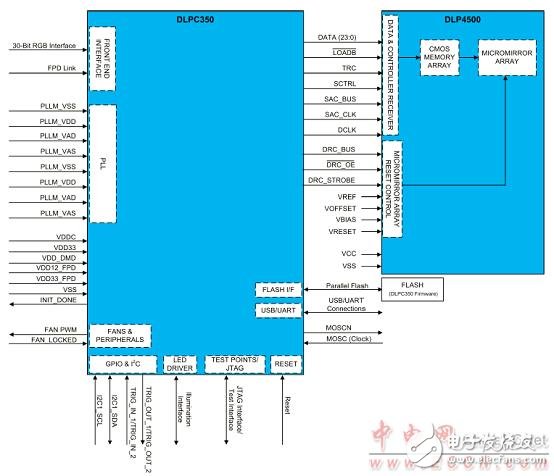
图1.DLP 0.45 WXGA芯片阻连接图
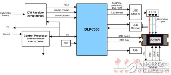
图2.典型系统框图
DLP 3D打印机
DLP 3-D Printer solutions process successive layers of material to produce a 3-D physical objects. The object is specified by a 3D Computer Aided Design (CAD) model. 3D printer software transforms the virtual 3D model into a series of layers suitable for printing the object.
It is often used to quickly create detailed prototypes. With this technology, printing parts of a material can be done in a single process flow. 3D printers are becoming more affordable for medium and small scale businesses in which rapid prototyping is brought all the way into the office, no longer requiring manufacturing floor space.
Two common methods for 3D printing are digital exposure and laser sintering. The high level principles for incorporating DLP technology into a 3D printing solution can be applied to both methods, but digital exposure is represented in the system block diagram.
For the digital exposure technique, the 3D object is constructed by laying down successive thin horizontal cross-sections or layers of an ultraviolet (UV) curable liquid photopolymer resin. For each layer, the UV light image from the DLP® Digital Micromirror Device (DMD) creates a pattern which hardens the polymer resin where it is exposed to the light.
The cross-section pattern is produced by the individual mirrors that correspond to each pixel on the current layer. This pattern projects through an imaging lens onto the surface of the UV curable liquid photopolymer resin, curing or hardening it where the pixels are on. As depicted in the diagram, one resin is the build material and the second is material to support overhanging features and thin vertical walls during construction. The support material is later removed by heat or dissolved with a solvent or water.
These layers fuse automatically and the process repeats one layer at a time until the model is built. Cure rates are possible under 0.2 seconds per layer. Layer thickness typically ranges from 1um to 250um based upon the resin and wavelength of the UV light used. More detailed images require more discrete cross-sections to assume the continuous smooth surface effect of the resulting object.
The diagram shows a DLP chipset, which includes the DMD, and a DMD Controller chip, plus a DMD Analog Control chip (depending on the specific DLP chipset). DLP chipsets are available with different DMD sizes, pixel pitches, resolutions, and other specifications. DLP also offers devices targeted for use with UV light. The best choice for a DLP chipset may depend on the desired object feature size, patterning speed and necessary wavelengths to cure the resin.
The CAD model is produced by software running on a PC. The system control and signal processing is accomplished by the Embedded Processor (Such as TI OMAP®). Power is provided by TI Power devices. The details of the optical layout and components are not shown in the diagram. The diagram is intended to convey as simply as possible the overall functionality of a DLP-based 3D Printer application. An actual product will require additional optical components and optical design in order to achieve full functionality.
DLP 3D打印机主要特性:
Integrated motor drive routine
Adaptive GUI for customizing layer sequences
Modular system design to port to other DLP chipsets
Block Diagram
Click on the colored blocks to view or sample recommended solutions
图3.DLP® LightCrafter™ 4500开发模块外形图
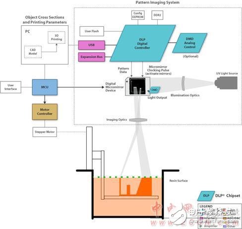
图4. DLP® LightCrafter™ 4500开发模块框图
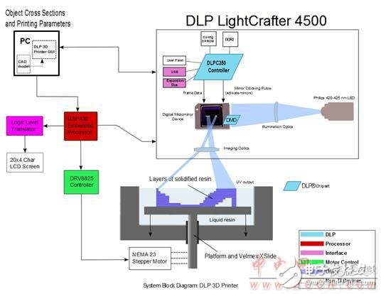
图5.DLP 3D打印机系统框图
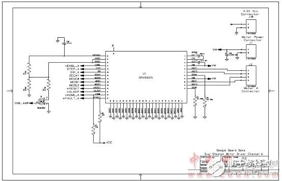
图6.DLP 3D打印机系统电路图(1)
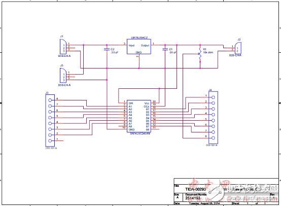
图7.DLP 3D打印机系统电路图(2)
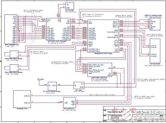
图8.DLP 3D打印机系统电路图(3)
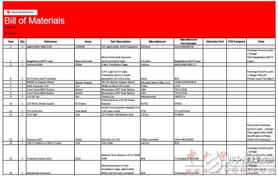
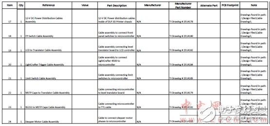
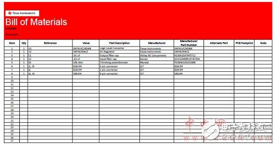
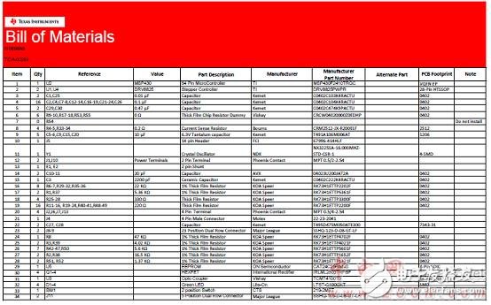
DLP 3D打印机系统材料清单:
- 相关推荐
- DLP4500
-
采用 DLP® 技术的顶级立体光固化成型印刷 3D 打印机2015-03-10 0
-
DLP4500使用问题2018-06-21 0
-
DLP4500与相机分辨率2018-06-23 0
-
DLP4500电源问题2018-06-23 0
-
dlp4500点云数据2018-08-29 0
-
采用DLP技术的欧特克Ember3D打印机2018-09-07 0
-
顶级立体光固化成型印刷3D打印机设计方案2018-10-12 0
-
购买 DLP4500的相关问题咨询2019-10-11 0
-
基于RK3399设计3D打印机方案2022-04-06 0
-
采用DLP® 技术的顶级立体光固化成型印刷3D打印机参考设计2022-09-26 0
-
使用DLP技术的3D打印2022-11-18 0
-
基于嵌入式Linux的桌面级DLP型3D打印机设计2018-03-06 1169
-
DLP 3D打印机总体框图介绍2018-04-04 10266
-
使用DLP设计桌面3D打印机的注意事项2021-10-19 2127
全部0条评论

快来发表一下你的评论吧 !
