

Lattice公司的DSP架构
汽车电子
描述
Lattice公司的ECP5/ECP5-5G系列FPGA具有高性能的特性如增强的DSP架构,高速SERDES和高速源同步接口,FPGA查找表达84K逻辑单元,高达365个I/O,并提供多达156个18x18乘法器和多种并行I/O标致.采用40nm工艺技术,非常适合量大高速和低成本的应用如汽车电子和智能监测等.本文介绍了ECP5/ECP5-5G系列FPGA主要特性,系列选择表,LFE5UM/LFE5UM5G-85器件简化框图以及嵌入视频开发套板,以及ECP5 VIP处理器板主要特性和电路图与材料清单.
The ECP5/ECP5-5G family of FPGA devices is optimized to deliver high performance features such as an enhanced DSP architecture, high speed SERDES and high speed source synchronous interfaces in an economical FPGA fabric. This combination is achieved through advances in device architecture and the use of 40 nm technology making the devices suitable for high-volume, high-speed, and low-cost applications.
The ECP5/ECP5-5G device family covers look-up-table (LUT) capacity to 84K logic elements and supports up to 365 user I/Os. The ECP5/ECP5-5G device family also offers up to 156 18 x 18 multipliers and a wide range of parallel I/O standards.
The ECP5/ECP5-5G FPGA fabric is optimized high performance with low power and low cost in mind. The ECP5/ ECP5-5G devices utilize reconfigurable SRAM logic technology and provide popular building blocks such as LUT-based logic, distributed and embedded memory, Phase Locked Loops (PLLs), Delay Locked Loops (DLLs), pre-engineered source synchronous I/O support, enhanced sysDSP slices and advanced configuration support, including encryption and dual-boot capabilities.
The pre-engineered source synchronous logic implemented in the ECP5/ECP5-5G device family supports a broad range of interface standards, including DDR2/3, LPDDR2/3, XGMII and 7:1 LVDS.
The ECP5/ECP5-5G device family also features high speed SERDES with dedicated Physical Coding Sublayer (PCS) functions. High jitter tolerance and low transmit jitter allow the SERDES plus PCS blocks to be configured to support an array of popular data protocols including PCI Express, Ethernet (XAUI, GbE, and SGMII) and CPRI. Transmit De-emphasis with pre- and post-cursors, and Receive Equalization settings make the SERDES suitable for transmission and reception over various forms of media.
The ECP5/ECP5-5G devices also provide flexible, reliable and secure configuration options, such as dual-boot capability, bit-stream encryption, and TransFR field upgrade features.
ECP5-5G family devices have made some enhancement in the SERDES compared to ECP5UM devices. These enhancements increase the performance of the SERDES to up to 5 Gb/s data rate.
The ECP5-5G family devices are pin-to-pin compatible with the ECP5UM devices. These allows a migration path for users to port designs from ECP5UM to ECP5-5G devices to get higher performance.
The Lattice Diamond™ design software allows large complex designs to be efficiently implemented using the ECP5/ECP5-5G FPGA family. Synthesis library support for ECP5/ECP5-5G devices is available for popular logic synthesis tools. The Diamond tools use the synthesis tool output along with the constraints from its floor planning tools to place and route the design in the ECP5/ECP5-5G device. The tools extract the timing from the routing and back-annotate it into the design for timing verification.
Lattice provides many pre-engineered IP (Intellectual Property) modules for the ECP5/ECP5-5G family. By using these configurable soft core IPs as standardized blocks, designers are free to concentrate on the unique aspects of their design, increasing their productivity.
ECP5 FPGA主要特性:
Higher Logic Density for Increased System Integration
12K to 84K LUTs
197 to 365 user programmable I/Os
Embedded SERDES
270 Mb/s, up to 3.2 Gb/s, SERDES interface(ECP5)
270 Mb/s, up to 5.0 Gb/s, SERDES interface (ECP5-5G)
Supports eDP in RDR (1.62 Gb/s) and HDR(2.7 Gb/s)
Up to four channels per device: PCI Express, Ethernet (1GbE, SGMII, XAUI), and CPRI
sysDSP™
Fullycascadable slice architecture
12 to 160 slices for high performance multiply and accumulate
Powerful 54-bit ALU operations
Time Division Multiplexing MAC Sharing
Rounding and truncation
Each slice supports
Half 36 x 36, two 18 x 18 or four 9 x 9 multipliers
Advanced 18 x 36 MAC and 18 x 18 Multiply-Multiply-Accumulate (MMAC) operations
Flexible Memory Resources
Up to 3.744 Mb sysMEM™ Embedded BlockRAM (EBR)
194K to 669K bits distributed RAM
sysCLOCK Analog PLLs and DLLs
Four DLLs and four PLLs in LFE5-45 and LFE5-85; two DLLs and two PLLs in LFE5-25 and LFE5-12
Pre-Engineered Source Synchronous I/O
DDR registers in I/O cells
Dedicated read/write levelling functionality
Dedicated gearing logic
Source synchronous standards support
ADC/DAC, 7:1 LVDS, XGMII
High Speed ADC/DAC devices
Dedicated DDR2/DDR3 and LPDDR2/LPDDR3 memory support with DQS logic, up to 800 Mb/s data-rate
Programmable sysI/O™ Buffer Supports Wide Range of Interfaces
On-chip termination
LVTTL and LVCMOS 33/25/18/15/12
SSTL 18/15 I, II
HSUL12
LVDS, Bus-LVDS, LVPECL, RSDS, MLVDS
subLVDS and SLVS, MIPI D-PHY input interfaces
Flexible Device Configuration
Shared bank for configuration I/Os
SPI boot flash interface
Dual-boot images supported
Slave SPI
TransFR™ I/O for simple field updates
Single Event Upset (SEU) Mitigation Support
Soft Error Detect – Embedded hard macro
Soft Error Correction – Without stopping user operation
Soft Error Injection – Emulate SEU event to debug system error handling
System Level Support
IEEE 1149.1 and IEEE 1532 compliant
Reveal Logic Analyzer
On-chip oscillator for initialization and general use
1.1 V core power supply for ECP5, 1.2 V core power supply for ECP5UM5G
ECP5和ECP5-5G系列选择表:
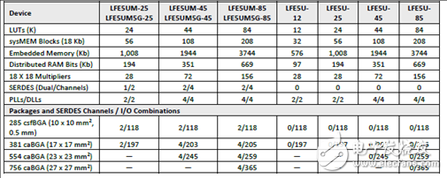
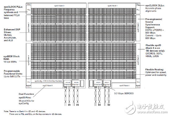
图1.LFE5UM/LFE5UM5G-85器件简化框图
嵌入视频开发套板
This kit is pre-programmed to demonstrate the Dual CSI-2 to HDMI demo. The dual camera inputs are received by the CrossLinkpASSP, which merges into a single video stream fed to the ECP5 FPGA. The ECP5 converts the incoming image into parallel data and also performs basic image processing, and then passes it to the HDMI VIP Output Bridge Board which converts the data to HDMI format. The output can be observed on a standard HDMI monitor.
嵌入视频开发套板包括:
Three-board connected kit consisting of:
Crosslink VIP Bridge Board
ECP5 VIP Processor Board
HDMI VIP Output Bridge Board
USB mini cable for programming
12V AC adaptor Power Supply
QuickStart Guide
Lattice Diamond software license request letter with unique serial number.
The following hardware is not included with this kit but required to complete this demo
HDMI-capable monitor
HDMI cable
图2.嵌入视频开发套板组合外形图
Embedded vision offers a promising future with many exciting new applications entering the market. These systems are used in industrial display systems for M2M applications and for Industry 4.0 implementations, Advanced Driver Assistance Systems (ADAS) and infotainment applications for automotive, DSLR cameras, drones, robotics, virtual reality (VR) systems, and medical equipment.
Lattice’s product portfolio offers flexible solutions to address today’s embedded vision designer’s needs, such as evolving interface requirements, energy-efficient image signal processing and hardware acceleration.
Let Lattice and its partners help you create flexible and power-efficient solutions for Embedded Vision Processing at the Edge.Embedded Vision Systems
The growing implementation of cameras in almost every industry contributes towards the creation of smarter machines. Concepts like object recognition, depth perception, collision avoidance and decision making are penetrating the devices in our homes, cities, factories and cars. Computing at the Edge requires a variety of devices working together to make the machines more efficient. Consumer, industrial and automotive industries are looking at FPGAs to help them create a flexible and intelligent learning environment to realize this future.
ECP5 VIP处理器板
This document describes the Lattice Semiconductor ECP5 VIP Processor Board which is a key component of Lattice’sVideo Interface Platform (VIP) board interconnect. Lattice VIP boards can be interconnected to create solutions forMIPI® CSI-2/DSI, SERDES, LVDS and more.
The content of this user guide includes descriptions of onboard jumper settings, programming circuit, a complete set ofschematics, and bill of materials for ECP5 VIP processor board.
ECP5 VIP处理器板主要特性:
ECP5/5G
SERDES interface
Dual DDR3 interface
LVDS/MIPI Transmitter/Receiver interface
SPI flash configuration
General Purpose Input/Output
Programming Circuit
Mini-B USB connector to FTDI
FTDI to ECP5 using JTAG
FTDI to ispClock using JTAG
ispClock
SERDES reference clock generation interface
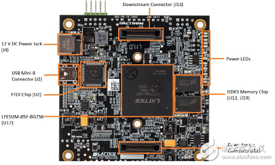
图3.ECP5 VIP处理器板外形图和主要元件(正面)
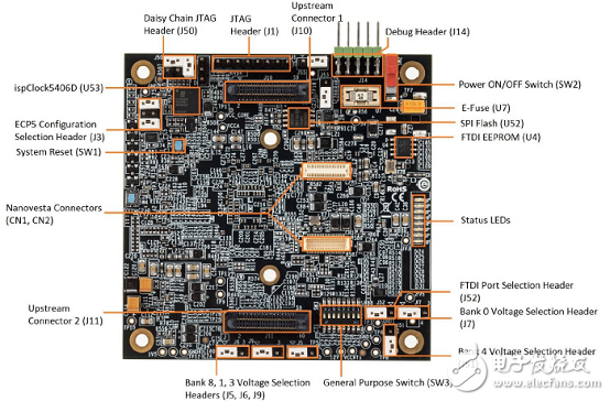
图4.ECP5 VIP处理器板外形图和主要元件(背面)
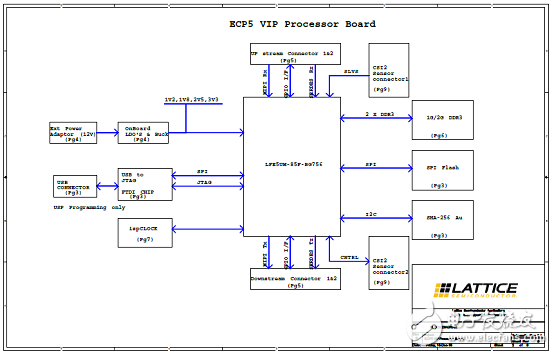
图5.ECP5 VIP处理器板框图
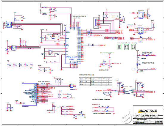
图6.ECP5 VIP处理器板电路图(1):FTDI和可编接口
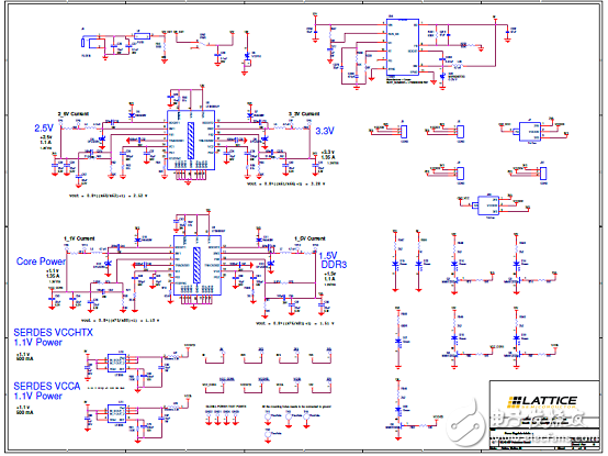
图7.ECP5 VIP处理器板电路图(2):电源稳压器接口
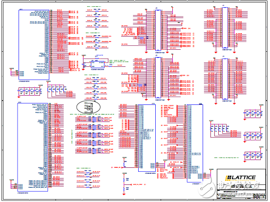
图8.ECP5 VIP处理器板电路图(3):MIPI和GPIO连接器接口
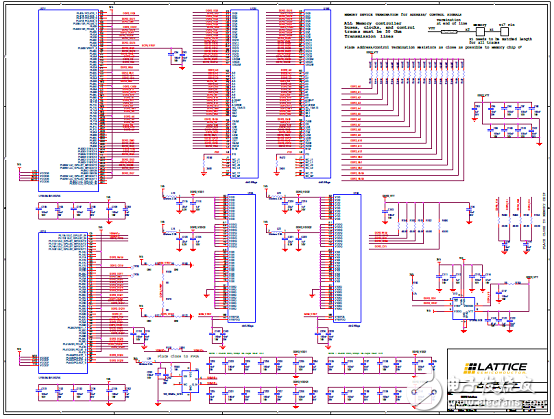
图9.ECP5 VIP处理器板电路图(4):DDR3接口
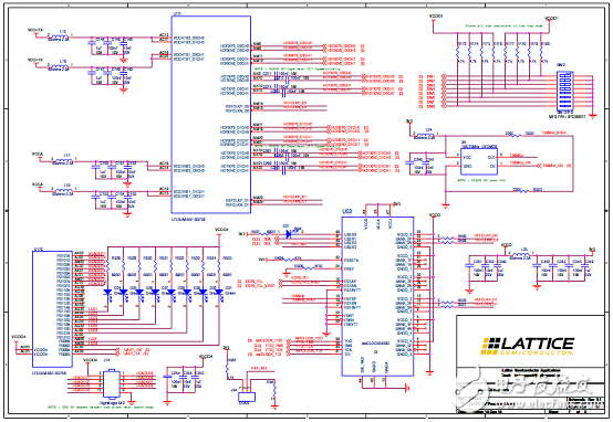
图10.ECP5 VIP处理器板电路图(5):SERDES接口
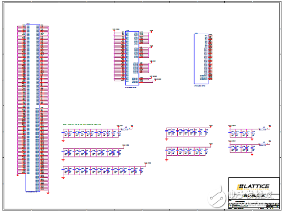
图11.ECP5 VIP处理器板电路图(6):ECP5去耦电容
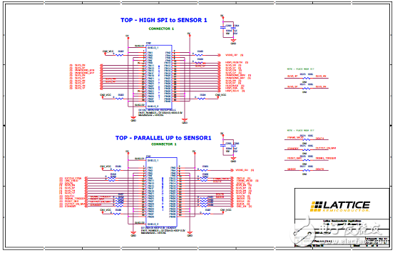
图12.ECP5 VIP处理器板电路图(7):HISPI/CSI2连接器
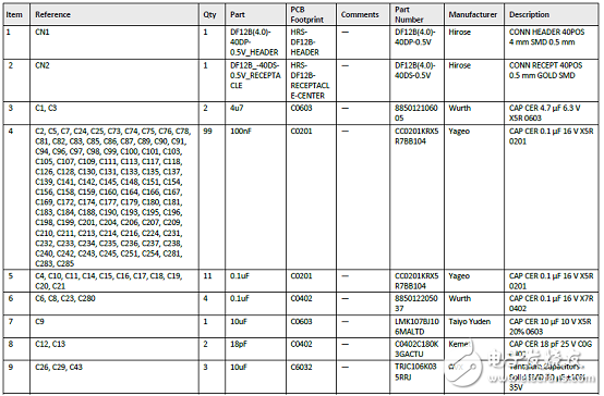
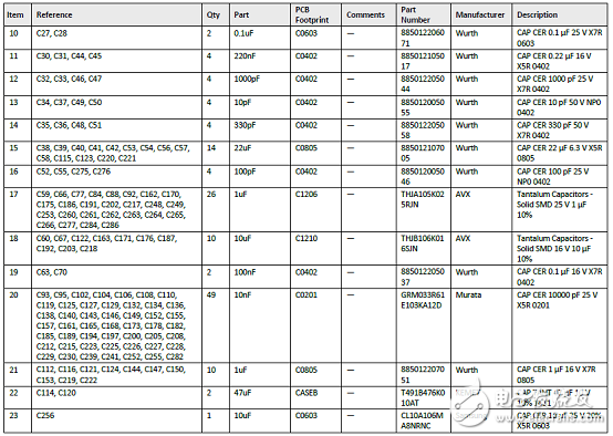
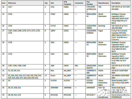
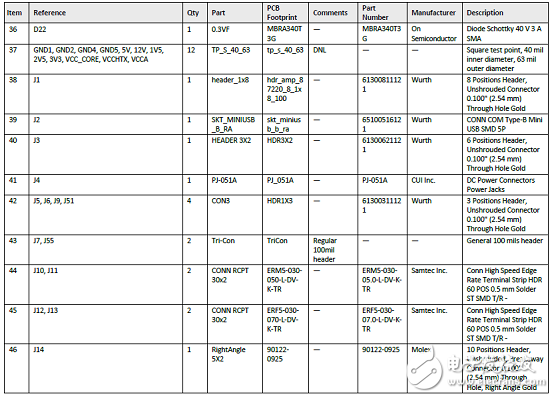
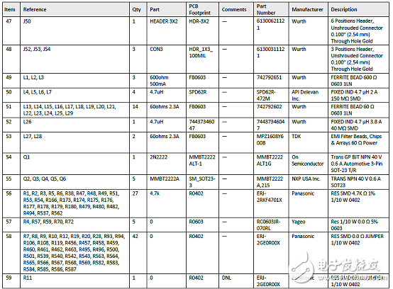
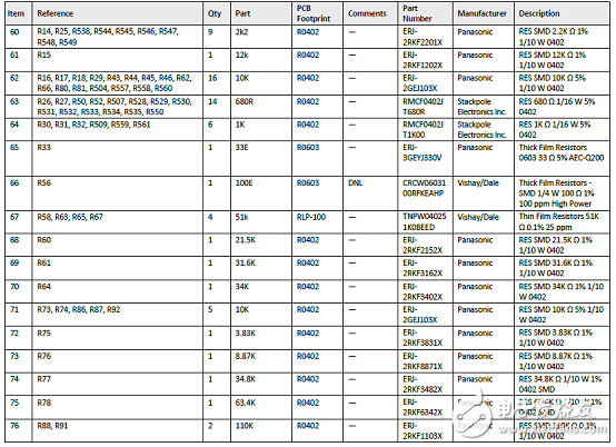
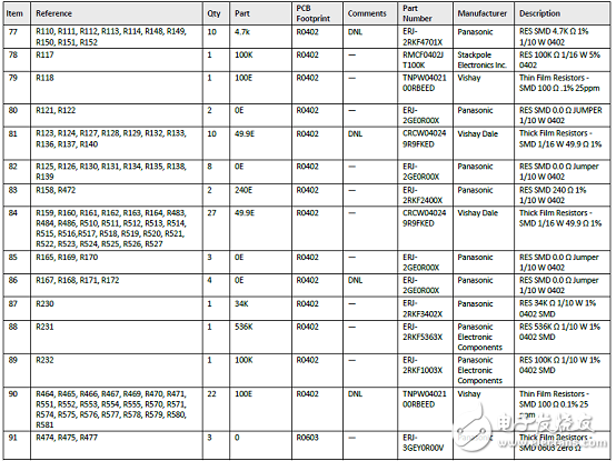
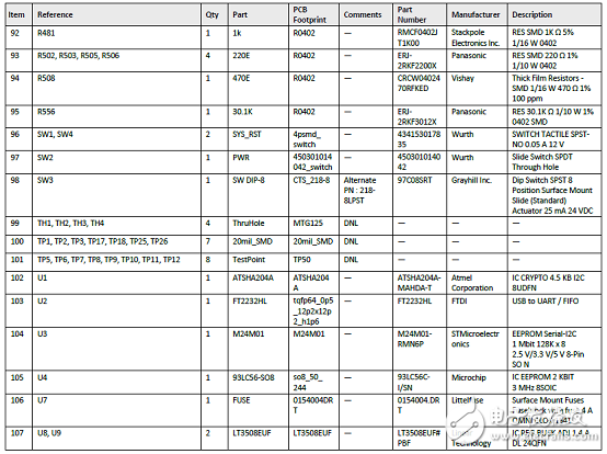
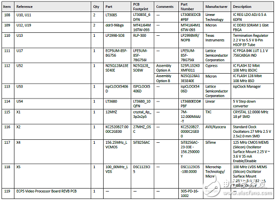
ECP5 VIP处理器板材料清单:
- 相关推荐
- 电路图
-
Lattice公司的系统内可编程PLD2009-06-20 1830
-
深圳公司招聘DSP高手1名2016-05-04 0
-
Lattice被收购 FPGA市场再次洗牌2016-12-07 0
-
请问有lattice FPGA的JTAG下载器相关资料吗?2019-04-25 0
-
新型DSP设计架构助力加速5G和AI开发2019-06-18 0
-
基于KeyStone架构的DSP电源设计方案2021-02-04 0
-
如何对ARM+DSP体系架构进行调试?2021-04-28 0
-
如何利用Lattice公司的可编程器件设计车用显示系统?2021-05-17 0
-
UltraScale DSP48 Slice架构的优势是什么?2021-05-24 0
-
Lattice LatticeMico32开发方案2009-11-24 525
-
LATTICE ispLEVER CLASSIC 1.2版设2008-08-28 1712
-
莱迪思半导体发布Lattice Diamond 1.4设计软件2011-12-14 1035
-
面对竞争 Lattice持续优化FPGA成本和功耗2012-08-14 790
-
Lattice公司FPGA产品三大定位2018-06-15 7950
-
了解UltraScale DSP架构如何降低设计功耗2018-11-29 2912
全部0条评论

快来发表一下你的评论吧 !
