

LPC8N04及LPC8N04开发板主要特性PCB设计图
电子技术
描述
NXP公司的LPC8N04是内置NFC接口的ARM Cortex-M0+ MCU,工作频率高达8MHz,内置了嵌套向量中断控制器(NVIC),ARM串行有线调试(SWD),具有NFC/RFID ISO 14443 type A接口,主要用在NFC控制的可配置LED串/圣诞树LED,智能玩具/交互机器人数据记录器,无接触控制板,无接触诊断,NFC电子锁,智能制造和NFC OTA.本文介绍了C主要特性和优势,框图,电源架构图以及LPC8N04开发板主要特性,电路图和PCB设计图.
The NXP LPC8N04 is an IC optimized for an entry level Cortex-M0+ MCU with built-in NFC interface. LPC8N04 supports an effective system solution with a minimal number of external components for NFC related applications.
The embedded ARM Cortex-M0+ offers flexibility to the users of this IC to implement their own dedicated solution. The LPC8N04 contains multiple features, including multiple power-down modes and a selectable CPU frequency of up to 8 MHz, for ultra-low power consumption.
Users can program this LPC8N04 with the industry-wide standard solutions for ARM Cortex-M0+ processors.
LPC8N04主要特性和优势:
System
ARM Cortex-M0+ processor running at frequencies of up to 8 MHz
ARM Cortex-M0+ built-in Nested Vectored Interrupt Controller (NVIC)
ARM Serial Wire Debug (SWD)
System tick timer
IC reset input
Memory
32 kB on-chip flash programming memory
4 kB on-chip EEPROM of which 256 byte can be write protected
8 kB SRAM
Digital peripherals
Up to 12 General Purpose Input Output (GPIO) pins with configurablepull-up/pull-down resistors and repeater mode
GPIO pins which can be used as edge and level sensitive interrupt sources
High-current drivers/sinks (20 mA) on four GPIO pins
High-current drivers/sinks (20 mA) on two I2C-bus pins
Programmable WatchDog Timer (WDT)
Analog peripherals
Temperature sensor with 1.5 C absolute temperature accuracy between 40 C
and +85 C
Communication interfaces
NFC/RFID ISO 14443 type A interface
I2C-bus interface supporting full I2C-bus specification and fast mode with a datarate of 400 kbit/s, with multiple address recognition and monitor mode
Energy harvesting functionality to power the LPC8N04.
Clock generation
8 MHz internal RC oscillator, trimmed to 2 % accuracy, which is used for thesystem clock
Timer oscillator operating at 32 kHz linked to the RTC timer unit
Power control
Support for 1.72 V to 3.6 V external voltages
The LPC8N04 can also be powered from the NFC field
Activation via NFC possible
Integrated Power Management Unit (PMU) for versatile control of powerconsumption
Four reduced power modes for ARM Cortex-M0+: sleep, deep sleep, deeppower-down and battery off
Power gating for each analog peripheral for ultra-low power operation
< 50 nA IC current consumption in battery off mode at 3.0 V
Power-On Reset (POR)
Unique device serial number for identification
LPC8N04应用:
Configurable LED strip/christmas tree LEDs via NFC
Smart toy/interactive robot data logger
Buttonless/contactless control panel
Contactless diagnostic
NFC e-locker
Smart manufacturing
NFC OTA
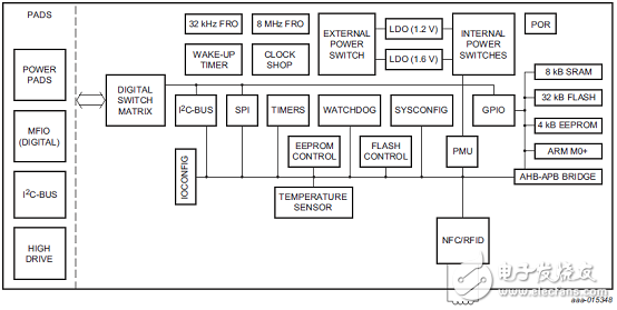
图1.LPC8N04框图
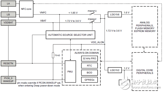
图2.LPC8N04电源架构图
LPC8N04开发板
The LPC8N04 Development Board board is developed by NXP to enable evaluation of and prototyping with the LPC8N04 MCU. Figure 3shows each side of LPC8N04 Development Board. The LPC8N04 device, buttons, jumpers and debug probe circuitry are on the top side (along with the board name). On the bottom side is a 5x7 array of LEDs, plus a surface mount speaker (LS1).
图3.LPC8N04开发板外形图
LPC8N04开发板主要特性:
• Compatible with MCUXpresso IDE and other popular toolchains (incl. IAR and Keil)
• Detachable, two-section board featuring minimal LPC8N04 system and debug probe /demo circuitry (LEDs and speaker)
• LPC8N04 Arm Cortex-M0+ MCU running at up to 8MHz
• Integrated NFC antenna
• Dual coin cell battery holders for
• On-board CMSIS-DAP (debug probe) with VCOM port, based on LPC11U35 MCU
• Debug connector to allow debug of target LPC8N04 MCU using an external probe
• LPC8N04 User button
• LPC8N04 Reset button
• 5x7 LED array for user applications
• Surface mounted speaker with amplifier
• Expansion connections with pin-outs compatible with I2C Grove and Pmodconnectors for easy connection of sensors
• Pre-programmed with demo message scrolling / tune playing application (requiresNFC-enabled phone to use; iOS 11 phones only support limited functionality)
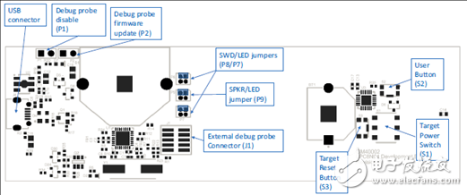
图4.LPC8N04开发板布局(顶层丝印)
图5.LPC8N04开发板电路图(1)
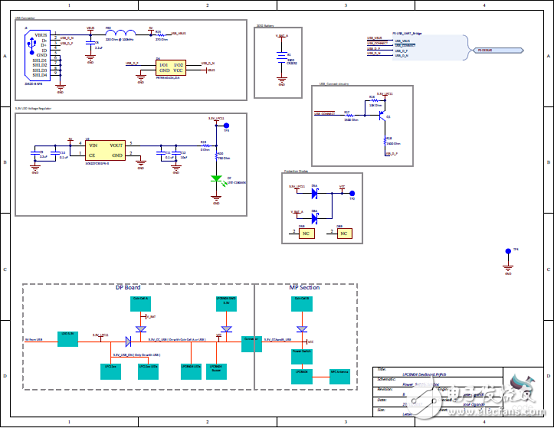
图6.LPC8N04开发板电路图(2)
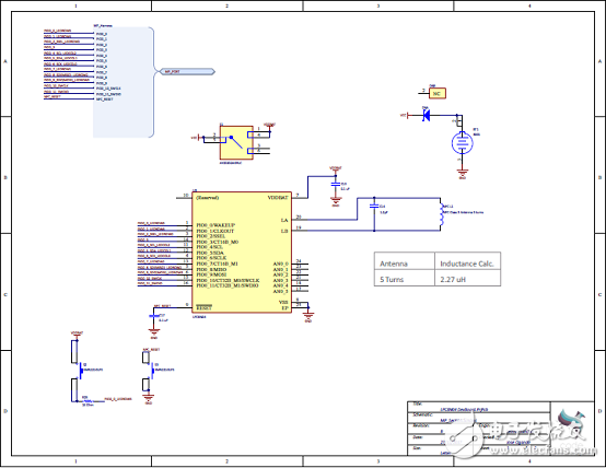
图7.LPC8N04开发板电路图(3)
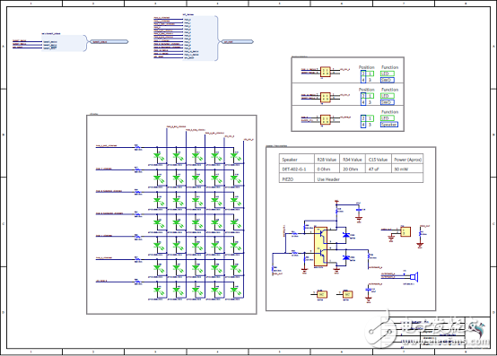
图8.LPC8N04开发板电路图(4)
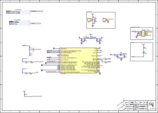
图9.LPC8N04开发板电路图(5)
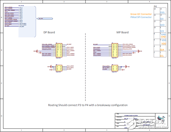
图10.LPC8N04开发板电路图(6)
图11.LPC8N04开发板PCB外形图(顶层)
图12.LPC8N04开发板PCB外形图(底层)
详情请见:
https://www.nxp.com/docs/en/data-sheet/LPC8N04.pdf?fsrch=1&sr=1&pageNum=1
和https://www.nxp.com/docs/en/user-guide/UM11082.pdf
UM11082.pdf
-
lpc2210开发板原理图2009-09-14 0
-
LPC800 开发板 电路图.pdf2016-09-19 0
-
开源咯~基于LPC8N04 MCU的物联网传感器节点设计方案(附硬件原理图,BOM清单和代码)2018-07-26 0
-
【看视频挖宝】NXP前沿技术抢先看,开发板、开发丛书、微信红包挖不停2018-11-21 0
-
LPC800系列LPC824介绍2019-09-23 0
-
LPC8N04快速数据手册2022-12-06 0
-
LPC8N04勘误表资料分享2022-12-06 0
-
集成NFC技术LPC8N04 MCU相关资料分享2022-12-09 0
-
LPC8N04开发板调试报错怎么解决?2023-04-12 0
-
LPC8N04如何重复使用的好的uart bitbash片段?2023-05-19 0
-
LPC8N04 I2C Master/Slave混合操作是否可行?2023-05-19 0
-
LPC8N04开发板的Daplink中的VCOM连到那里了?2023-11-08 0
-
LPC1768开发板的特性及USB通信应用方案的研究2019-07-16 3888
-
LPC8N04 勘误表2022-12-07 66
全部0条评论

快来发表一下你的评论吧 !
