

ECP5-5G及ECP5-5G Versa开发板主要特性
汽车电子
描述
Lattice公司的ECP5-5G系列是低成本低功耗小尺寸的FPGA系列产品,提供高性能特性如增强的DSP架构,高速SERDES和高速源同步接口,以及高达84K逻辑单元的查找表(LUT),支持高达365个用户I/O,高达156个18 x 18乘法器和各种并行I/O标准,特别适合用在量大高速低成本的应用如汽车娱乐系统,小型无线基站和低功耗工业视频照相机.本文介绍了ECP5-5G主要特性,框图和ECP5-5G Versa开发板主要特性,电路图和材料清单.
The ECP5/ECP5-5G family of FPGA devices is optimized to deliver high performance features such as an enhanced DSP architecture, high speed SERDES and high speed source synchronous interfaces in an economical FPGA fabric. This combination is achieved through advances in device architecture and the use of 40 nm technology making the devices suitable for high-volume, high-speed, low-cost applications.
The ECP5/ECP5-5G device family covers look-up-table (LUT) capacity to 84K logic elements and supports up to 365 user I/Os. The ECP5/ECP5-5G device family also offers up to 156 18 x 18 multipliers and a wide range of parallel I/O standards.
The ECP5/ECP5-5G FPGA fabric is optimized high performance with low power and low cost in mind. The ECP5/ ECP5-5G devices utilize reconfigurable SRAM logic technology and provide popular building blocks such as LUT-based logic, distributed and embedded memory, Phase Locked Loops (PLLs), Delay Locked Loops (DLLs), pre-engineered source synchronous I/O support, enhanced sysDSP slices and advanced configuration support, including encryption and dual-boot capabilities.
The pre-engineered source synchronous logic implemented in the ECP5/ECP5-5G device family supports a broad range of interface standards, including DDR2/3, LPDDR2/3, XGMII and 7:1 LVDS.
The ECP5/ECP5-5G device family also features high speed SERDES with dedicated Physical Coding Sublayer (PCS) functions. High jitter tolerance and low transmit jitter allow the SERDES plus PCS blocks to be configured to support an array of popular data protocols including PCI Express, Ethernet (XAUI, GbE, and SGMII) and CPRI. Transmit De-emphasis with pre- and post-cursors, and Receive Equalization settings make the SERDES suitable for transmission and reception over various forms of media.
The ECP5/ECP5-5G devices also provide flexible, reliable and secure configuration options, such as dual-boot capability, bit-stream encryption, and TransFR field upgrade features.
ECP5-5G family devices have made some enhancement in the SERDES compared to ECP5UM devices. These enhancements increase the performance of the SERDES to up to 5 Gb/s data rate.
The ECP5-5G family devices are pin-to-pin compatible with the ECP5UM devices. These allows a migration path for users to port designs from ECP5UM to ECP5-5G devices to get higher performance.
The Lattice Diamond™ design software allows large complex designs to be efficiently implemented using the ECP5/ECP5-5G FPGA family. Synthesis library support for ECP5/ECP5-5G devices is available for popular logic synthesis tools. The Diamond tools use the synthesis tool output along with the constraints from its floor planning tools to place and route the design in the ECP5/ECP5-5G device. The tools extract the timing from the routing and back-annotate it into the design for timing verification.
Lattice provides many pre-engineered IP (Intellectual Property) modules for the ECP5/ECP5-5G family. By using these configurable soft core IPs as standardized blocks, designers are free to concentrate on the unique aspects of their design, increasing their productivity.
ECP5-5G主要特性:
• Higher Logic Density for Increased System Integration
• 12K to 84K LUTs
• 197 to 365 user programmable I/Os
• Embedded SERDES
• 270 Mb/s, up to 3.2 Gb/s,SERDES interface(ECP5)
• 270 Mb/s, up to 5.0 Gb/s,SERDES interface (ECP5-5G)
• Supports eDP in RDR (1.62 Gb/s) and HDR(2.7 Gb/s)
• Up to four channels per device: PCI Express, Ethernet(1GbE,SGMII,XAUI),and CPRI
• sysDSP™
• Fully cascadable slice architecture
• 12 to 160 slices for high performance multiply and accumulate
• Powerful 54-bit ALU operations
• Time Division Multiplexing MAC Sharing
• Rounding and truncation
• Each slice supports • Half 36 x 36, two 18 x 18 or four 9 x 9 multipliers
• Advanced 18 x 36 MAC and 18 x 18 Multiply-Multiply-Accumulate (MMAC) operations
• Flexible Memory Resources
• Up to 3.744 Mb sysMEM™ Embedded Block RAM (EBR)
• 194K to 669K bits distributed RAM
• sysCLOCK Analog PLLs and DLLs
Four DLLs and four PLLs in LFE5-45 and LFE5-85; two DLLs and two PLLs in LFE5-25 and LFE5-12
• Pre-Engineered Source Synchronous I/O
• DDR registers in I/O cells
• Dedicated read/write levelling functionality
• Dedicated gearing logic
• Source synchronous standards support • ADC/DAC, 7:1 LVDS, XGMII
• High Speed ADC/DAC devices
• Dedicated DDR2/DDR3 and LPDDR2/LPDDR3 memory support with DQS logic, up to 800 Mb/s data-rate
• Programmable sysI/O™ Buffer Supports Wide Range of Interfaces
• On-chip termination
• LVTTL and LVCMOS 33/25/18/15/12
• SSTL 18/15 I, II
• HSUL12
• LVDS, Bus-LVDS, LVPECL, RSDS, MLVDS
subLVDS and SLVS, MIPI D-PHY input interfaces
• Flexible Device Configuration
• Shared bank for configuration I/Os
• SPI boot flash interface
• Dual-boot images supported
• Slave SPI
• TransFR™ I/O for simple field updates
• Single Event Upset (SEU) Mitigation Support
• Soft Error Detect – Embedded hard macro
• Soft Error Correction – Without stopping user operation
• Soft Error Injection – Emulate SEU event to debug system error handling
• System Level Support
• IEEE 1149.1 and IEEE 1532 compliant
• Reveal Logic Analyzer
• On-chip oscillator for initialization and general use
• 1.1 V core power supply
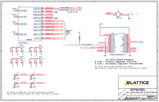
图1. ECP5-5G简化框图: LFE5UM/LFE5UM5G-85
ECP5-5G主要特性:
Up to 3.2 Gbps SERDES rate with ECP5, and up to 5 Gbps with ECP5-5G
Up to 4 channels per device in dual channel blocks for higher granularity
Enhanced DSP blocks provide 2x resource improvement for symmetrical filters
Single event upset (SEU) mitigation support Programmable IO support for LVCMOS 33/25/18/15/12, XGMII, LVTTL, LVDS, Bus-LVDS, 7:1 LVDS, LVPECL and MIPI D-PHY input interfaces
ECP5-5G Versa开发板
The ECP5-5G™ Versa Development Board allows designers to investigate and experiment with the features of the ECP5-5G Field-Programmable Gate Array. The features of the ECP5-5G Versa Development Board can assist engineers with rapid prototyping and testing of their specific designs. The ECP5-5G Versa Development Board is part of the ECP5-5G Versa Development Kit. The guide is intended to be referenced in conjunction with demo user guides to demonstrate the ECP5-5G FPGA.
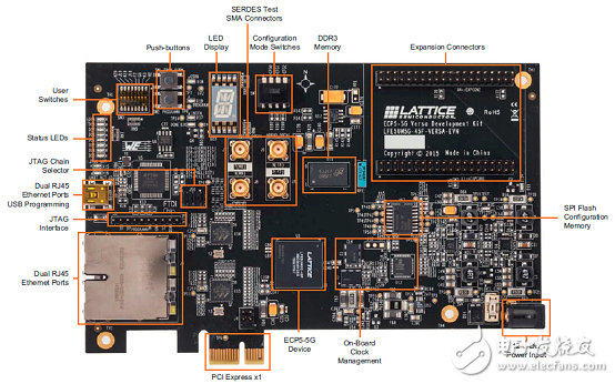
图2. ECP5-5G Versa开发板外形图
ECP5-5G Versa开发板主要特性:
• Half-length PCI Express form-factor
— Allows demonstration of PCI Express x1 interconnection
• Electrical testing of one full-duplex SERDES channel via SMA connections
• USB-B connection for UART and device programming
• Two RJ45 interfaces to 10/100/1000 Ethernet to RGMII
• On-board Boot Flash
— 128M Serial SPI Flash
• DDR3-1866 memory components (64Mb/x16)
• Expansion mezzanine interconnection for prototyping
• 14-segment alpha-numeric display
• Switches, LEDs and displays for demo purposes
• Diamond® programming support
• On-board reference clock sources
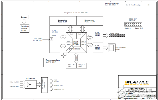
图3.ECP5-5G Versa开发板框图
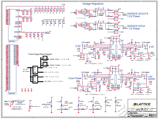
图4.ECP5-5G Versa开发板电路图:电压稳压器
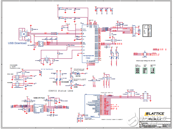
图5.ECP5-5G Versa开发板电路图:编程
图6.ECP5-5G Versa开发板电路图:SERDES
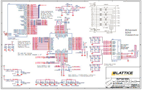
图7.ECP5-5G Versa开发板电路图:10/100/1000-T PHY #1/RJ45
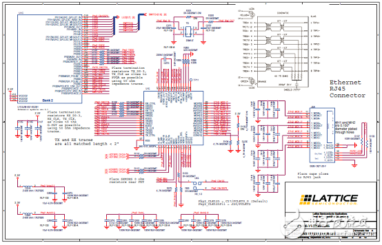
图8.ECP5-5G Versa开发板电路图:10/100/1000-T PHY #2/RJ45
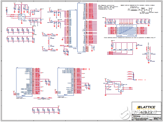
图9.ECP5-5G Versa开发板电路图:DDR3存储器
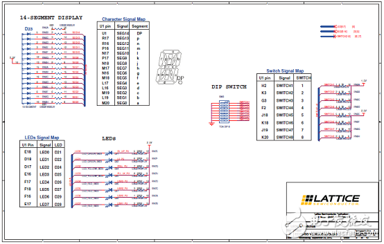
图10.ECP5-5G Versa开发板电路图:LED和开关
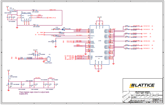
图11.ECP5-5G Versa开发板电路图:参考时钟发生器
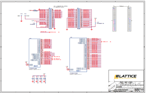
图12.ECP5-5G Versa开发板电路图:扩展连接器
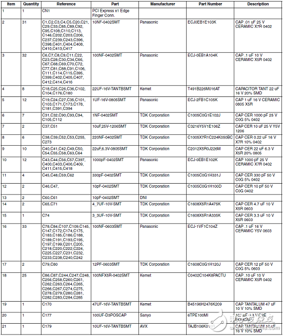
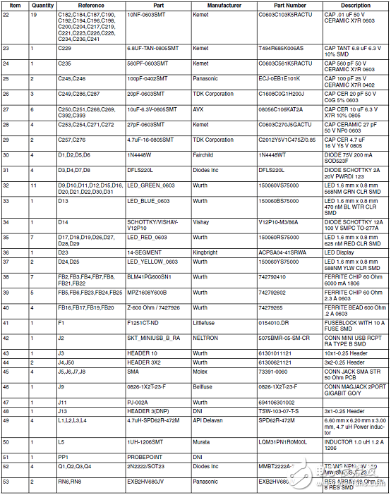
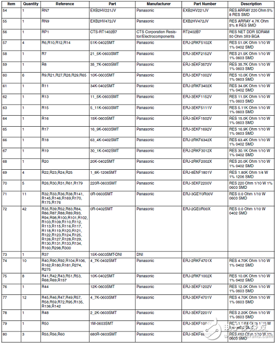
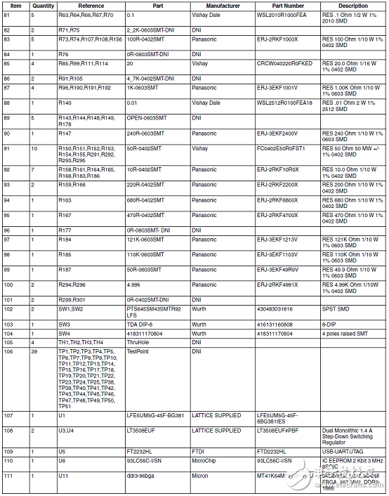
ECP5-5G Versa开发板材料清单:
详情请见:
和
DS1044.pdf
ECP5-5GVersaDevKitQS039.pdf
-
#硬声创作季 #5G 5G通行行业现状学习电子知识 2022-11-01
-
#硬声创作季 #5G 5G行业驱动力及行业前景分析学习电子知识 2022-11-01
-
#硬声创作季 #5G 5G基本概念及应用场景学习电子知识 2022-11-01
-
初步认识5G天线#硬声创作季 #5G学习电子知识 2022-11-01
-
5G应用数据采集#硬声创作季 #5G学习电子知识 2022-11-01
-
[6.4.1]--5-2-2越区覆盖问题处理#硬声创作季 #5G 5G应用网络优化学习电子知识 2022-11-01
-
[6.6.1]--5-3-25G应用导频污染问题处理视频#硬声创作季 #5G学习电子知识 2022-11-01
-
5G 网络智能化运营运维#硬声创作季 #5G学习电子知识 2022-11-01
-
[5.7.2]--5G关键技术和应用场景#硬声创作季 #5G学习电子知识 2022-11-02
-
4G/5G全系列安卓智模块开发板jf_87063710 2023-12-18
-
如何使用ECP5FPGA解决网络边缘应用设计挑战2020-10-21 0
-
Lattice ECP5和ECP5-5G FPGA系列VIP处理器解决方案2018-04-06 11774
-
对Lattice ECP3/ECP5器件中的SerDes/PCS进行了简要的介绍2018-06-13 7154
-
基于全新ECP5-5G器件的IP和解决方案, 适用于工业和通信应用2018-07-31 1327
-
Lattice ECP3/ECP5器件中的SerDes/PCS简要介绍2018-08-16 11164
全部0条评论

快来发表一下你的评论吧 !
