

ADI ADAQ7980 16位ADC μModule 数据采集系统解决方案
电子说
描述
ADI公司的ADAQ7980/ADAQ7988是16位模数转换器(ADC) μModule® 数据采集系统,集成了四个常见信号处理和调理模块,采用支持各种应用的系统级封装(SiP)设计。内置一个高精度低功耗16位SAR ADC,一个低功耗高带宽高输入阻抗ADC驱动器,一个稳定的低功耗基准电压缓冲器和一个高效的电源管理模块,可简化数据采集系统的设计过程。主要用在自动测试设备(ATE),电池供电仪器仪表,通信,数据采集,过程控制和医疗仪器。本文介绍了ADAQ7980主要特性,框图,以及评估板EVAL-ADAQ7980SDZ主要特性,简化框图,电路图,材料清单和PCB设计图。
The ADAQ7980/ADAQ7988 are 16-bit analog-to-digital converter (ADC) μModule® data acquisition systems that integrate four common signal processing and conditioning blocks into a system in package (SiP) design that supports a variety of applications. These devices contain the most critical passive components, eliminating many of the design challenges associated with traditional signal chains that use successive approximation register (SAR) ADCs. These passive components are crucial to achieving the specified device performance.
The ADAQ7980/ADAQ7988 contain a high accuracy, low power, 16-bit SAR ADC, a low power, high bandwidth, high input impedance ADC driver, a low power, stable reference buffer, and an efficient power management block. Housed within a tiny, 5 mm × 4 mm LGA package, these products simplify the design process for data acquisition systems. The level of system integration of the ADAQ7980/ADAQ7988 solves many design challenges, while the devices still provide the flexibility of a configurable ADC driver feedback loop to allow gain and/or common-mode adjustments.A set of four device supplies provides optimal system performance; however,single-supply operation is possible with minimal impact on device operating specifications. The ADAQ7980/ADAQ7988 integrate within a compact, integrated circuit (IC)-like form factor key components commonly used in data acquisition signal chain designs. The μModule family transfers the design burden of component selection,optimization, and layout from designer to device, shortening overall design time, system troubleshooting, and ultimately improving time to market. The serial peripheral interface (SPI)-compatible serial interface features the ability to daisy-chain multiple devices on a single, 3- wire bus and provides an optional busy indicator. The user interface is compatible with 1.8 V, 2.5 V, 3 V, or 5 V logic. Specified operation of these devices is from −55℃ to +125℃。
ADAQ7980主要特性:
Easy to use
μModule data acquisition system
All active components designed by Analog Devices, Inc.
50% PCB area savings
Includes critical passive components
SPI-/QSPI-/MICROWIRE™-/DSP-compatible serial interface
Daisy-chain multiple ADAQ7980/ADAQ7988 devices
Versatile supply configuration with 1.8 V/2.5 V/3 V/5 V logic interface
High performance
16-bit resolution with no missing codes
Throughput: 1 MSPS (ADAQ7980) and 500 kSPS (ADAQ7988)
INL: ±8 ppm typical and 20 ppm maximum
SNR: 91.5 dB typical at 10 kHz (unity gain)
THD: −105 dB at 10 kHz Zero error: ±0.06 mV typical (unity gain)
Zero error temperature drift: 1.3 μV/°C maximum
Low power dissipation
21 mW typical at 1 MSPS (ADAQ7980)
16.5 mW typical at 500 kSPS (ADAQ7988)
Flexible power-down modes
Small, 24-lead, 5 mm × 4 mm LGA package
Excellent ESD ratings
3500 V human body model (HBM)
1250 V field-induced charged device model (FICDM)
Wide operating temperature range: −55℃ to +125℃
ADAQ7980应用:
Automated test equipment (ATE)
Battery powered instrumentation
Communications
Data acquisition
Process control
Medical instruments
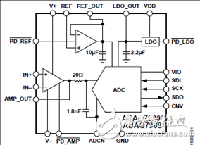
图1.ADAQ7980功能框图
评估板EVAL-ADAQ7980SDZ
The EVAL-ADAQ7980SDZ is an evaluation board designed to demonstrate the low power ADAQ7980 performance and provide an easy to understand interface for a variety of system applications. The ADAQ7980 is a 16-bit, 1 MSPS, μModule data acquisition system that integrates four common signal processing and conditioning blocks into a system in package (SiP) design that supports a variety of applications.
The EVAL-ADAQ7980SDZ can also evaluate the ADAQ7988, despite being populated with the ADAQ7980. To mimic the evaluation of the ADAQ7988 performance, limit the maximum sample rate of the ADAQ7980 to 500 kSPS in the ADAQ798x Evaluation Software.
The evaluation board is ideal for use with the Analog Devices, Inc., system demonstration platform (SDP) board, EVAL-SDP-CB1Z. The EVAL-ADAQ7980SDZ interfaces to the SDP board via a 120-pin connector. P1, P2, P3, and P4 SMA connectors are provided to connect a low noise analog signal source.
The ADAQ798x Evaluation Software executable controls the evaluation board over the USB through the EVAL-SDP-CB1Z. See the Related Links section for a list of on-board components.
A full description and complete specifications for the ADAQ7980 are provided in the ADAQ7980/ADAQ7988 data sheet and must be consulted in conjunction with this user guide when using the evaluation board. Full details on the EVAL-SDP-CB1Z are available on the SDP-B product page.
评估板EVAL-ADAQ7980SDZ主要特性:
Full featured evaluation board for the ADAQ7980
Versatile analog signal conditioning circuitry
On-board reference, reference buffers, and ADC drivers
SDP board-compatible (EVAL-SDP-CB1Z)
PC software for control and data analysis of time and frequency domain
评估板EVAL-ADAQ7980SDZ包括:
EVAL-ADAQ7980SDZ evaluation board
Wall power supply 9 V dc adapter
Daughter card power connector
Nylon screws
图2.评估板EVAL-ADAQ7980SDZ外形图
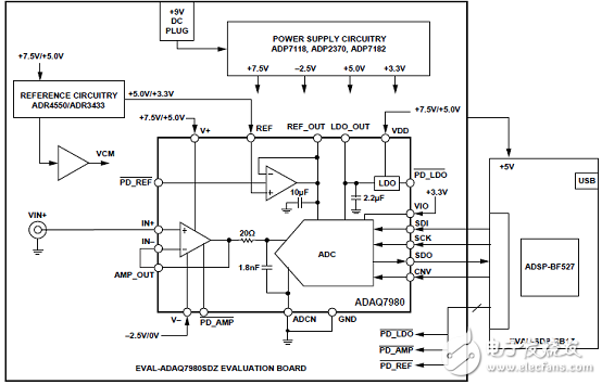
图3.评估板EVAL-ADAQ7980SDZ简化框图
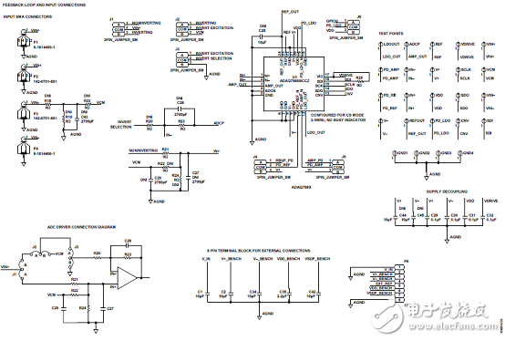
图4.评估板EVAL-ADAQ7980SDZ电路图(1)
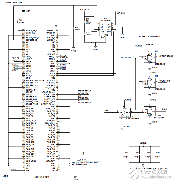
图5.评估板EVAL-ADAQ7980SDZ电路图(2)
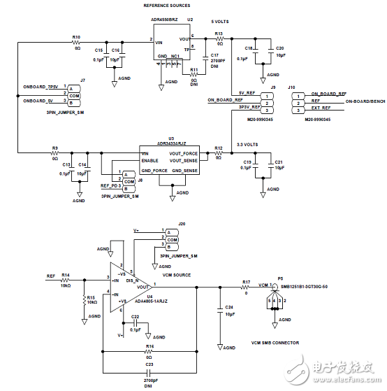
图6.评估板EVAL-ADAQ7980SDZ电路图(3)
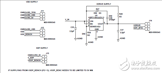
图7.评估板EVAL-ADAQ7980SDZ电路图(4)
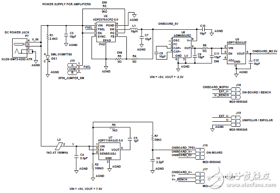
图8.评估板EVAL-ADAQ7980SDZ电路图(5)
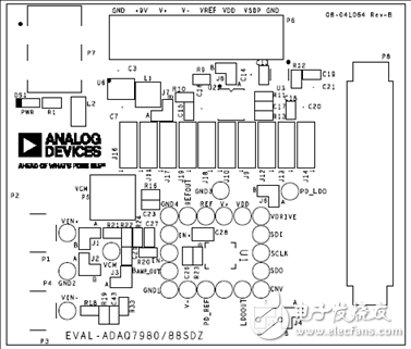
图9.评估板EVAL-ADAQ7980SDZ PCB设计图:顶层丝印-装配
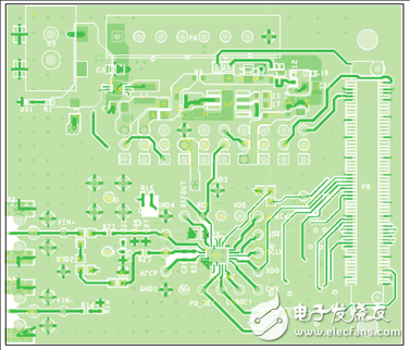
图10.评估板EVAL-ADAQ7980SDZ PCB设计图:顶层
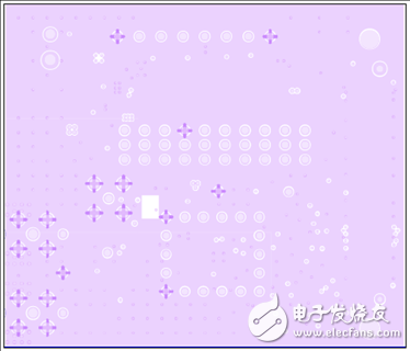
图11.评估板EVAL-ADAQ7980SDZ PCB设计图:层层叠2-地
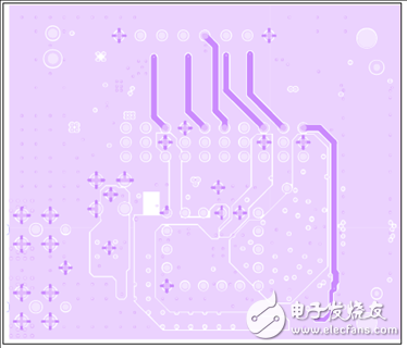
图12.评估板EVAL-ADAQ7980SDZ PCB设计图:层3-电源
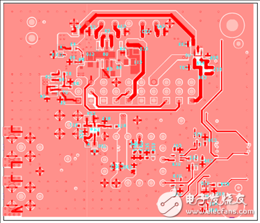
图13.评估板EVAL-ADAQ7980SDZ PCB设计图:底层
-
请问ADAQ7980/88中单电源5V供电时,模拟输入电压范围为0.15V~VREF吗?2018-07-30 0
-
全能DAQ ADAQ798x增加单极性输入的增益配置2018-10-11 0
-
基于SiP技术提高精密数据采集信号链密度2018-10-19 0
-
16通道,24位ΔΣADC,为数据采集提供小巧灵活和精确的解决方案2019-07-12 0
-
全能ADC的使用2019-07-24 0
-
关于ADAQ7980/88中单电源5V供电时,模拟输入电压的问题求解2023-11-17 0
-
DAQ ADAQ798x为何要配置ADC驱动器?2023-12-11 0
-
μModule精密数据采集ADAQ4003的功能特点及应用范围2020-11-30 962
-
Arrow, AnalogMax-DAQ2, featuring ADAQ79802021-01-30 403
-
ADAQ7980/ADAQ7988 IBIS Model2021-02-20 341
-
UG-1533:评估ADAQ4003 18位2 MSPSµ模块数据采集解决方案2021-03-22 464
-
ADAQ7980ADAQ7988 IBIS型号2021-06-02 360
-
基于EVAL-ADAQ7980SDZ数据采集系统的参考设计2021-07-09 376
-
ADAQ系列µModule百科全“课”开播!2022-12-19 438
-
ADAQ4380-4:四、16比、4 MSPS、同声抽样、微模数据采集初步数据表 ADI2023-10-11 21
全部0条评论

快来发表一下你的评论吧 !
