

FM0-64L-S6E1C3主要特性和,系统框图解析
控制/MCU
描述
cypress公司的FM0-64L-S6E1C3系列是高读集成的32位MCU,设计用于低功耗和低成本的嵌入式控制器.器件具有集成了片上闪存和SRAM的ARMCortex-M0+处理器,还包含了各种定时器,ADC和各种通信接口(UART,CSIO(SPI),I2C,I2S,智能卡和USB)等在内的外设功能.工作频率高达40.8MHz.本文介绍了FM0-64L-S6E1C3系列产品主要特性,框图,以及FM0-64L-S6E1C3 MCU入门开发板主要特性和元件分布图,系统框图,电路图,材料清单和PCB设计文件.
The S6E1C3 Series is a series of highly integrated 32-bit microcontrollers designed for embedded controllers aiming at low powerconsumption and low cost. This series has the ARM Cortex-M0+ Processor with on-chip Flash memory and SRAM, and consists ofperipheral functions such as various timers, ADC and communication interfaces (UART, CSIO (SPI), I2C, I2S, Smart Card, and USB).
The products which are described in this data sheet are placed into TYPE3-M0+ product categories in "FM0+ Family PeripheralManual".
FM0-64L-S6E1C3主要特性:
32-bit ARM Cortex-M0+ Core
Processor version: r0p1
Maximum operating frequency: 40.8 MHz
Nested Vectored Interrupt Controller (NVIC): 1 NMI(non-maskable interrupt) and 24 peripheral interrupt with 4selectable interrupt priority levels
24-bit System timer (Sys Tick): System timer for OS taskmanagement
Bit Band Operation
Compatible with Cortex-M3 bit band operation.
On-Chip Memory
Flash memory
Up to 128 Kbytes
Read cycle: 0 wait-cycle
Security function for code protection
SRAM
The on-chip SRAM of this series has one independent SRAM .
Up to 16 Kbytes
4Kbytes: can retain value in Deep standby Mode
USB Interface
USB interface is composed of Device and Host
With Main PLL, USB clock can be generated by multiplicationof Main clock.
USB Device
USB 2.0 Full-Speed supported
Max 6 EndPoint supported
• EndPoint 0 is control transfer
• EndPoint 1, 2 can be selected Bulk-transfer,Interrupt-transfer or Isochronous-transfer
• EndPoint 3 to 5 can select Bulk-transfer orInterrupt-transfer
• EndPoint 1 to 5 comprise Double Buffer
• The size of each EndPoint is according to the follows
• EndPoint 0, 2 to 5 : 64 bytes
• EndPoint1 : 256 bytes
USB host
USB 2.0 Full/Low-Speed supported
Bulk-transfer, Interrupt-transfer and Isochronous-transfersupport
USB Device connected/disconnected automatically detect
IN/OUT token handshake packet automatically
Max 256-byte packet-length supported
Wake-up function supported
Multi-Function Serial Interface (Max 6channels)
3 channels with 64Byte FIFO (Ch.4, 6 and 7), 3 channelswithout FIFO (Ch.0, 1 and 3)
The operation mode of each channel can be selected fromone of the following.
UART
CSIO (CSIO is known to many customers as SPI)
I2C
UART
Full duplex double buffer
Parity can be enabled or disabled.
Built-in dedicated baud rate generator
External clock available as a serial clock
Hardware Flow control* : Automatically control thetransmission by CTS/RTS (only ch.4)
* : S6E1C32B0A/S6E1C31B0A andS6E1C32C0A/S6E1C31C0A do not support HardwareFlow control.
Various error detection functions (parity errors, framingerrors, and overrun errors)
CSIO (also known as SPI)
Full duplex double buffer
Built-in dedicated baud rate generator
Overrun error detection function
Serial chip select function (ch1 and ch6 only)
Data length: 5 to 16 bits
I2C
Standard-mode (Max: 100 kbps) supported / Fast-mode(Max 400 kbps) supported.
I2S (MFS-I2S)
Using CSIO (Max 2 ch: ch.4, ch.6) and I2S clock generator
Supports two transfer protocol
• I2S
• MSB-justified
Master mode only
I2C Slave
I2C Slave supports the slave function of I2C and wake-upfunction from Standby mode.
Descriptor System Data Transfer Controller (DSTC)(64 Channels)
The DSTC can transfer data at high-speed without going viathe CPU. The DSTC adopts the Descriptor system and,following the specified contents of the Descriptor that hasalready been constructed on the memory, can access directlythe memory / peripheral device and performs the datatransfer operation.
It supports the software activation, the hardware activation,and the chain activation functions
A/D Converter (Max: 8 Channels)
12-bit A/D Converter
Successive approximation type
Conversion time: 2.0 μs @ 2.7 V to 3.6 V
Priority conversion available (2 levels of priority)
scan conversion mode
Built-in FIFO for conversion data storage (for scanconversion: 16 steps, for priority conversion: 4 steps)
Base Timer (Max: 8 Channels)
The operation mode of each channel can be selected from oneof the following.
16-bit PWM timer
16-bit PPG timer
16/32-bit reload timer
16/32-bit PWC timer
General-Purpose I/O Port
This series can use its pin as a general-purpose I/O port whenit is not used for an external bus or a peripheral function. Allports can be set to fast general-purpose I/O ports or slowgeneral-purpose I/O ports. In addition, this series has a portrelocate function that can set to which I/O port a peripheralfunction can be allocated.
All ports are Fast GPIO which can be accessed by 1cycle
Capable of controlling the pull-up of each pin
Capable of reading pin level directly
Port relocate function
Up to 54 fast general-purpose I/O ports @64-pin package
Certain ports are 5 V tolerant.
Dual Timer (32-/16-bit Down Counter)
The Dual Timer consists of two programmable 32-/16-bit downcounters. The operation mode of each timer channel can beselected from one of the following.
Free-running mode
Periodic mode (= Reload mode)
One-shot mode
Real-Time Clock
The Real-time Clock countsyear/month/day/hour/minute/second/day of the week from year00 to year 99.
The RTC can generate an interrupt at a specific time(year/month/day/hour/minute/second/day of the week) andcan also generate an interrupt in a specific year, in a specificmonth, on a specific day, at a specific hour or at a specific
minute.
It has a timer interrupt function generating an interrupt upona specific time or at specific intervals.
It can keep counting while rewriting the time.
It can count leap years automatically.
Watch Counter
The Watch Counter wakes up the microcontroller from the lowpower consumption mode. The clock source can be selectedfrom the main clock, the sub clock, the built-in high-speed CRclock or the built-in low-speed CR clock.
Interval timer: up to 64 s (sub clock: 32.768 kHz)
External Interrupt Controller Unit
Up to 12 external interrupt input pins
Non-maskable interrupt (NMI) input pin: 1
Watchdog Timer (2 Channels)
The watchdog timer generates an interrupt or a reset when thecounter reaches a time-out value.This series consists of two different watchdogs, hardwarewatchdog and software watchdog.
The hardware watchdog timer is clocked by the built-inlow-speed CR oscillator. Therefore, the hardware watchdog isactive in any low-power consumption modes except RTC, Stop,
Deep standby RTC and Deep standby Stop mode.
CRC (Cyclic Redundancy Check) Accelerator
The CRC accelerator calculates the CRC which has a heavysoftware processing load, and achieves a reduction of theintegrity check processing load for reception data and storage.
CCITT CRC16 and IEEE-802.3 CRC32 are supported.
CCITT CRC16 Generator Polynomial: 0x1021
IEEE-802.3 CRC32 Generator Polynomial: 0x04C11DB7
HDMI-CEC/Remote Control Receiver (Up to 2Channels)
HDMI-CEC transmitter
Header block automatic transmission by judging Signalfree
Generating status interrupt by detecting Arbitration lost
Generating START, EOM, ACK automatically to outputCEC transmission by setting 1 byte data
Generating transmission status interrupt when transmitting1 block (1 byte data and EOM/ACK)
HDMI-CEC receiver
Automatic ACK reply function available
Line error detection function available
Remote control receiver
4 bytes reception buffer
Repeat code detection function available
Smart Card Interface (Max 1 Channel)
Compliant with ISO7816-3 specification
Card Reader only/B class card only
Available protocols
Transmitter: 8E2, 8O2, 8N2
Receiver: 8E1, 8O1, 8N2, 8N1, 9N1
Inverse mode
TX/RX FIFO integrated (RX: 16-bytes, TX:16-bytes)
Clock and Reset
Clocks
A clock can be selected from five clock sources (two externaloscillators, two built-in CR oscillator, and main PLL).
Main clock: 8 MHz to 48 MHz
Sub clock: 32.768 kHz
Built-in high-speed CR clock: 8 MHz
Built-in low-speed CR clock: 100 kHz
Main PLL clock 8MHz to 16MHz (Input),75MHz to 150MHz (Output)
Resets
Reset request from the INITX pin
Power on reset
Software reset
Watchdog timer reset
Low-voltage detection reset
Clock supervisor reset
Clock Supervisor (CSV)
The Clock Supervisor monitors the failure of external clockswith a clock generated by a built-in CR oscillator.
If an external clock failure (clock stop) is detected, a reset isasserted.
If an external frequency anomaly is detected, an interrupt ora reset is asserted.
Low-Voltage Detector (LVD)
This series monitors the voltage on the VCC pin with a 2-stagemechanism. When the voltage falls below a designated voltage,the Low-voltage Detector generates an interrupt or a reset.
LVD1: monitor VCC and error reporting via an interrupt
LVD2: auto-reset operation
Low Power Consumption Mode
This series has six low power consumption modes.
Sleep
Timer
RTC
Stop
Deep standby RTC (selectable between keeping the value ofRAM and not)
Deep standby Stop (selectable between keeping the value ofRAM and not)
Peripheral Clock Gating
The system can reduce the current consumption of the totalsystem with gating the operation clocks of peripheral functionsnot used.
Debug
Serial Wire Debug Port (SW-DP)
Micro Trace Buffer (MTB)
Unique ID
A 41-bit unique value of the device has been set.
Power Supply
Wide voltage range:
VCC = 1.65V to 3.6 V
VCC = 3.0V to 3.6V (when USB is used)
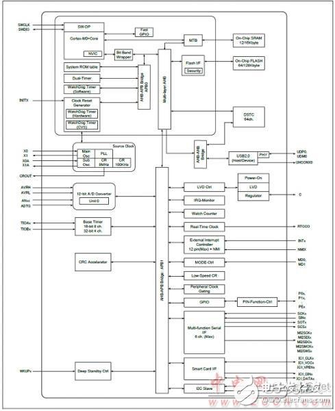
图1.FM0-64L-S6E1C3功能框图表
The FM0-64L-S6E1C3 MCU Starter Kit is a low cost development platform for Cypress’s FM0+ S6E1C-Series, a Flexible Microcontroller family with an ultra-low-power 32-bit ARM® Cortex®-M0+ CPU. This kit enables rapid development of embedded systems with onboard interfaces including USB, digital audio and an Arduino™ Uno-compatible form-factor to prototype with Arduino shields.
图2.FM0-64L-S6E1C3 MCU入门开发板外形图
FM0-64L-S6E1C3 MCU入门开发板主要特性:
Featuring the FM0+ S6E1C-Series: ARM® Cortex-M0+ MCU
40MHz ARM® Cortex-M0+ MCU with 64-channel DMA
128KB flash, 16KB SRAM and 54 GPIOs
Industry’s most efficient 35µA/CoreMark® Score
Ultra-low-power consumption: Active - 40µA/MHz and Standby - 1.2µA
Advanced peripherals: USB host and device, HDMI-CEC and 6x Serial Interfaces
FM0-64L-S6E1C3 MCU入门开发板包括:
FM0+ S6E1C-Series Starter Board
USB Standard-A to Micro-B cable
Quick Start Guide
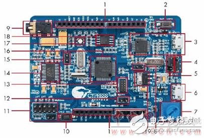
图3.FM0-64L-S6E1C3 MCU入门开发板主要元件分布图
1. Arduino Interface (CN7-CN10)
2. User button
3. MB9AF312K programmer and debugger (CMSIS-DAP)
4. Serial programming mode select (J3)
5. Power supply resource select (J4)
6. USB device connector (CN4)
7. Potentiometer
8. MB9AF312K programming mode jumper (J1)
9. Headphone and microphone jack (CN1)
10. Reset button
11. Multicon connector (CN12, CN13)
12. Jumper for current measurement (J5)
13. 10-pin JTAG connector
14. Stereo codec
15. Programming mode jumper (J2)
16. Cypress FM0+ MCU S6E1C32D0A
17. RGB LED
18. NOR flash
19. 3.3 V voltage regulator
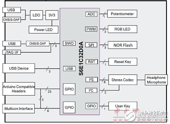
图4.FM0-64L-S6E1C3 MCU入门开发板系统框图
硬件主要特性:
Cypress FM0+ S6E1C-Series MCU
On-board ICE (CMSIS-DAP compatible)
USB device interface
Potentiometer
NOR flash memory
Stereo codec
RGB LED
User button
Arduino compatible headers
Multicon interface
图5.FM0-64L-S6E1C3 MCU入门开发板电路图(1)
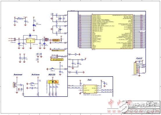
图6.FM0-64L-S6E1C3 MCU入门开发板电路图(2)
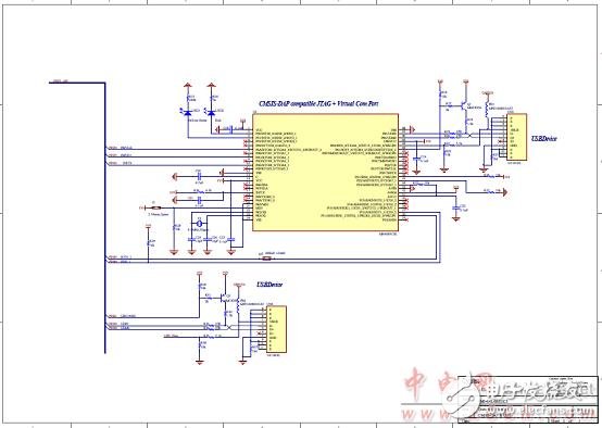
图6.FM0-64L-S6E1C3 MCU入门开发板电路图(2)
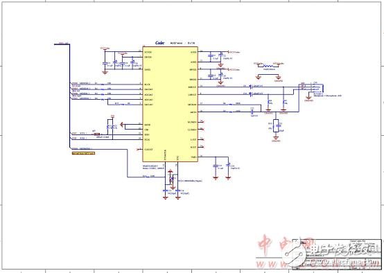
图7.FM0-64L-S6E1C3 MCU入门开发板电路图(3)
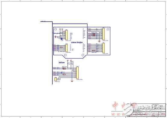
图8.FM0-64L-S6E1C3 MCU入门开发板电路图(4)
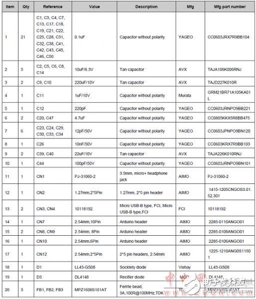
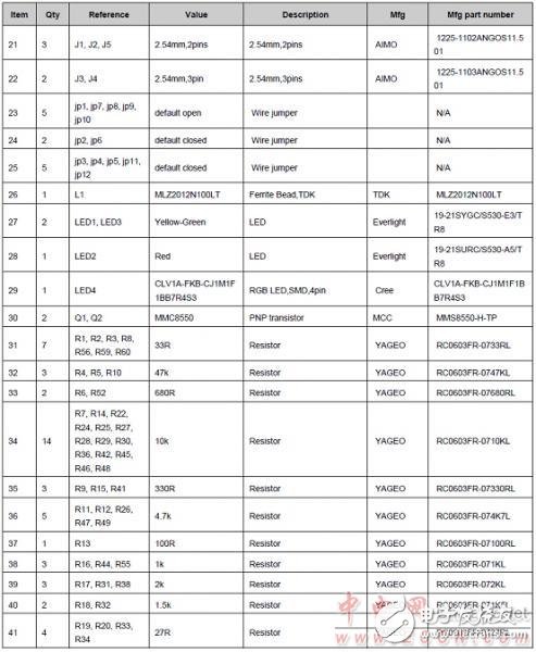
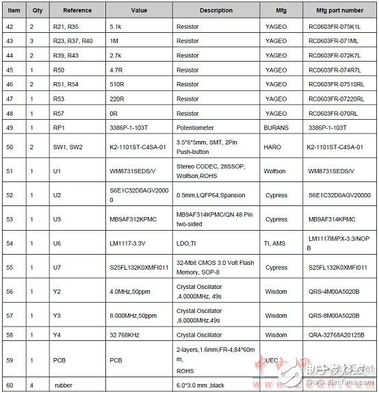
FM0-64L-S6E1C3 MCU入门开发板材料清单:
-
S6E1C3能否产生重复启动?2024-01-30 0
-
秋叶系统Ghost Win8.1 UP3 X64纯净版v2017.062017-06-21 0
-
FM4-176l-s6e2cc支持w5500以太网模块吗2018-11-07 0
-
FM4 S6E2CC是否需要额外下载到PDL?2019-01-04 0
-
S6E1C3 SWD/JTAG通信故障该怎么办?2019-10-21 0
-
劳易测传感器IS 212FM4NO.5F-6E0-S122020-06-04 0
-
SICK西克SAS4-S060N3PS1T0D2020-09-14 0
-
霍尼韦尔变送器STG74L-E1G000-1-C-BHS-11C-A-60A0-00-00002021-04-22 0
-
霍尼韦尔差压变送器STD820-E1AC4AS-1-A-AHC-11C-A-10A62021-05-11 0
-
霍尼韦尔变送器STD810-E1AC4AS-1-0-AHB-11S2021-05-11 0
-
时钟系统框图解读2021-08-19 0
-
VL53L1CBV0FY/1、CBTL1616A0UK、BCM43598XKUBGT、LTM4644MPY、MSC8328Q、STM32L011E4Y6TR 回收物料2021-11-15 0
-
FM4 S6E2C系列主要特性和框图2018-04-22 2394
-
基于FM0-64L-S6E1C3微控制器的参考设计2021-07-09 342
全部0条评论

快来发表一下你的评论吧 !

