

ADI公司ADSP-BF54x处理器开发方案介绍
嵌入式技术
描述
ADI 公司的ezLINX iCoupler绝缘接口开发平台采用ADSP-BF54x Blackfin系列处理器,用来评估八种物理层数字绝缘的通信标准(USB, RS-422, RS-485, RS-232, CAN, SPI, I2C 和LVDS),由于Blackfin ADSP-BF548处理器运行在uCLinux操作系统,很容易通过开源硬件和软件平台实现个性化,大大缩短了开发时间,ezLINX上的接口ezLINX采用ADI的绝缘收发器.本文介绍了ADSP-BF54x主要特性,方框图,ezLINX iCoupler绝缘接口开发平台主要特性,框图,电路图和材料清单.
The ADSP-BF54x Blackfin® processors are members of the Blackfin family of products, incorporating the Analog Devices/ Intel Micro Signal Architecture (MSA). Blackfin processors combine a dual-MAC state-of-the-art signal processing engine, the advantages of a clean, orthogonal RISC-like microprocessor instruction set, and single-instruction, multiple-data (SIMD) multimedia capabilities into a single instruction-set Architecture.
LOW POWER ARCHITECTURE
Blackfin processors provide world-class power management and performance. Blackfin processors are designed in a low power and low voltage design methodology and feature on-chip dynamic power management, the ability to vary both the voltage and frequency of operation to significantly lower overall power consumption. Reducing both voltage and frequency can result in a substantial reduction in power consumption as compared to reducing only the frequency of operation. This translates into longer battery life for portable appliances.
SYSTEM INTEGRATION
The ADSP-BF54x Blackfin processors are highly integrated system-on-a-chip solutions for the next generation of embedded network connected applications. By combining industrystandard interfaces with a high performance signal processing core, users can develop cost-effective solutions quickly without the need for costly external components. The system peripherals include a high speed USB OTG (On-the-Go) controller with integrated PHY, CAN 2.0B controllers, TWI controllers, UART ports, SPI ports, serial ports (SPORTs), ATAPI controller, SD/SDIO controller, a real-time clock, a watchdog timer, LCD controller, and multiple enhanced parallel peripheral interfaces.
BLACKFIN PROCESSOR PERIPHERALS
The ADSP-BF54x processors contain a rich set of peripherals connected to the core via several high bandwidth buses, providing flexibility in system configuration as well as excellent overall system performance . The general purpose peripherals include functions such as UARTs, SPI, TWI, timers with pulse width modulation (PWM) and pulse measurement capability, general-purpose I/O pins, a real-time clock, and a watchdog timer. This set of functions satisfies a wide variety of typical system support needs and is augmented by the system expansion capabilities of the part. The ADSPBF54x processors contain dedicated network communication modules and high speed serial and parallel ports, an interrupt controller for flexible management of interrupts from the onchip peripherals or external sources, and power management control functions to tailor the performance and power characteristics of the processor and system to many application scenarios.
All of the peripherals, except for general-purpose I/O, CAN, TWI, real-time clock, and timers, are supported by a flexible DMA structure. There are also separate memory DMA channels dedicated to data transfers between the processor’s various memory spaces, including external DDR (either standard or mobile, depending on the device) and asynchronous memory.
Multiple on-chip buses running at up to 133 MHz provide enough bandwidth to keep the processor core running along with activity on all of the on-chip and external peripherals.
The ADSP-BF54x Blackfin processors include an on-chip voltage regulator in support of the dynamic power management capability. The voltage regulator provides a range of core voltage levels when supplied from VDDEXT. The voltage regulator can be bypassed at the user’s discretion.
ADSP-BF54x主要特性:
Up to 600MHz high performance Blackfin processor
Two 16-bit MACs, two 40-bit ALUs, four 8-bit video ALUs
RISC-like register and instruction model
Wide range of operating voltages and flexible booting options
Programmable on-chip voltage regulator
400-ball CSP_BGA, RoHS compliant package
MEMORY
Up to 324K bytes of on-chip memory comprised of instruction SRAM/cache; dedicated instruction SRAM; data SRAM/cache; dedicated data SRAM; scratchpad SRAM
External sync memory controller supporting either DDR
SDRAM or mobile DDR SDRAM
External async memory controller supporting 8-/16-bit async memories and burst flash devices
NAND flash controller
4 memory-to-memory DMA pairs, 2 with ext. requests
Memory management unit providing memory protection
Code security with Lockbox secure technology and 128-bit
AES/ARC4 data encryption
One-time-programmable (OTP) memory
PERIPHERALS
High speed USB On-the-Go (OTG) with integrated PHY
SD/SDIO controller
ATA/ATAPI-6 controller
Up to 4 synchronous serial ports (SPORTs)
Up to 3 serial peripheral interfaces (SPI-compatible)
Up to 4 UARTs, two with automatic H/W flow control
Up to 2 CAN (controller area network) 2.0B interfaces
Up to 2 TWI (2-wire interface) controllers
8- or 16-bit asynchronous host DMA interface
Multiple enhanced parallel peripheral interfaces (EPPIs), supporting ITU-R BT.656 video formats and 18-/24-bit LCD connections
Media transceiver (MXVR) for connection to a MOST network
Pixel compositor for overlays, alpha blending, and color conversion
Up to eleven 32-bit timers/counters with PWM support
Real-time clock (RTC) and watchdog timer
Up/down counter with support for rotary encoder
Up to 152 general-purpose I/O (GPIOs)
On-chip PLL capable of frequency multiplication
Debug/JTAG interface
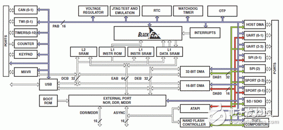
图1.ADSP-BF549功能框图
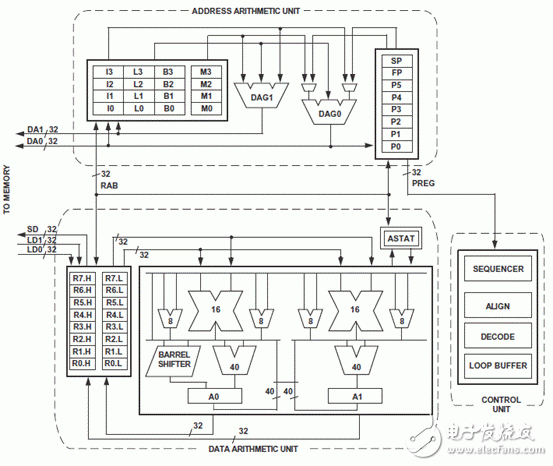
图2.Blackfin处理器核框图
ezLINX iCoupler绝缘接口开发平台
The ezLINX iCoupler Isolated Interface Development environment provides developers with a cost-effective, plug and play method for evaluating eight physical Layer, digitally-isolated communication standards(USB, RS-422, RS-485, RS-232, CAN, SPI, I2C and LVDS). The Blackfin ADSP-BF548 processor is used to run the uCLinux operating system and allows for easy customization through the open source hardware and software platform. Development time is significantly reduced for embedded designers and system architects who are designing and evaluating isolated communication standards.The Interfaces on ezLINX use ADI’s isolated transceivers with integrated iCoupler and isoPower® digital isolator technology.
图3.ezLINX iCoupler绝缘接口开发平台外形图
The Hardware of the ezLINX iCoupler isolated interface development environment contains the ADSP-BF548 blackfin processor with 64MB of RAM and 32MB of Flash memory. The Isolated Physical layer communication standards are implemented using ADI’s isolated transceivers with integrated iCoupler and isoPower technology. Routing between the various communication standards is implemented at the hardware level.
ezLINX iCoupler绝缘接口开发平台包括:
Isolated USBusing the ADuM3160
Isolated CANusing the ADM3053 Signal and Power Isolated CAN transceiver
Isolated RS-485/RS-422using the ADM2587E Signal and Power Isolated RS-485/RS-422 transceiver
Isolated RS-232using the ADM3252E Signal and Power Isolated RS-232 transceiver
Isolated I2Cusing the ADuM1250 and ADuM5000
Isolated SPIusing the ADuM3401, ADuM3402 and ADuM5000
Isolated LVDSusing the ADuM3442, ADuM5000, ADN4663 and ADN4664
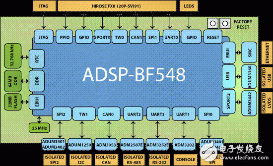
图4.ezLINX iCoupler绝缘接口开发平台方框图
The ezLINX™ Development Platform also includes the following:
Hirose FX8 120P-SV(91) Extender Connectorfor daughter board connections.
RS-232 DB-9 Console Connector
1.2V, 2.5V, 3.3V, 5V Regulated Output Voltages
ADSP-BF548 Isolated Transceivers EvalBoard
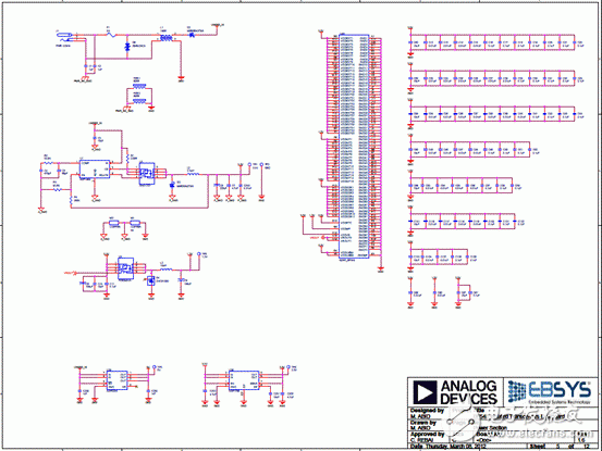
图5.ezLINX iCoupler绝缘接口开发平台电路图(1)
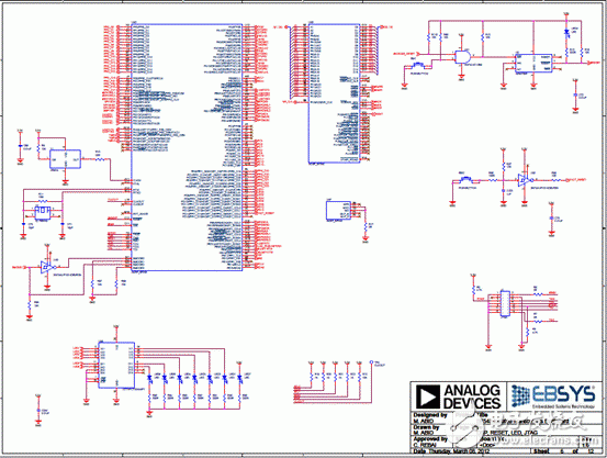
图6.ezLINX iCoupler绝缘接口开发平台电路图(2)
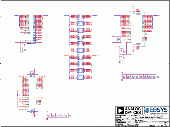
图7.ezLINX iCoupler绝缘接口开发平台电路图(3)
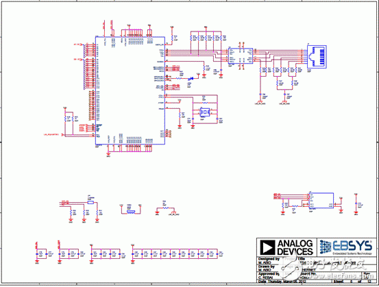
图8.ezLINX iCoupler绝缘接口开发平台电路图(4)
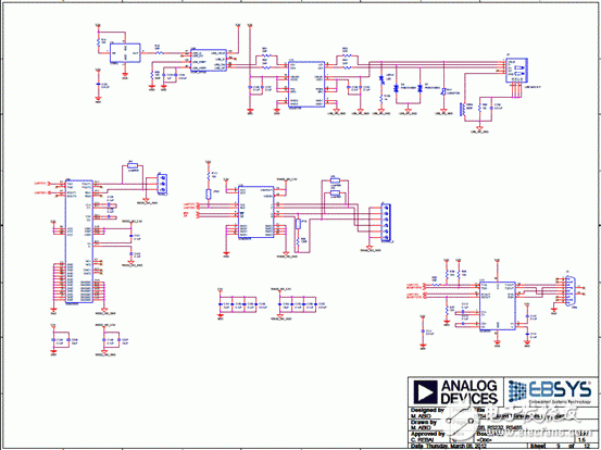
图9.ezLINX iCoupler绝缘接口开发平台电路图(5)
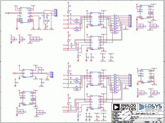
图10.ezLINX iCoupler绝缘接口开发平台电路图(6)
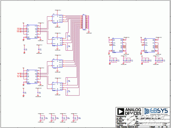
图11.ezLINX iCoupler绝缘接口开发平台电路图(7)
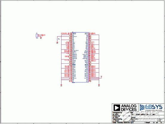
图12.ezLINX iCoupler绝缘接口开发平台电路图(7)
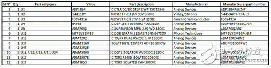
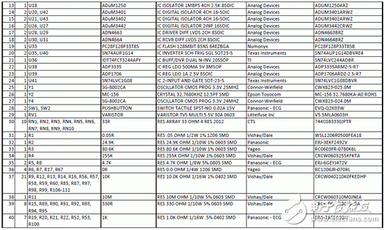
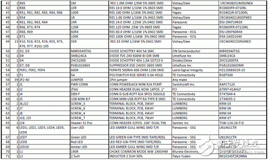
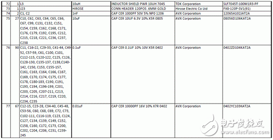
ezLINX iCoupler绝缘接口开发平台材料清单:
-
ADI SHARC处理器有哪些应用案例2018-10-31 0
-
Blackfin处理器ADZS-BF707-EZLITE,ADSP-BF70x EZ-KIT Lite评估系统2019-03-13 0
-
adsp bf54x资料2019-04-29 0
-
Blackfin ADSP-BF70x系列DSP处理器,业界性能领先的超低功耗DSP解决方案2019-08-21 0
-
评估双核Blackfin处理器的ADZS-BF609-EZLITE ADSP-BF609 EZ-KIT Lite评估系统2020-03-13 0
-
一文解析BF518F Blackfin处理器开发评估方案2018-05-12 4354
-
ADSP-BF542/ADSP-BF544/ADSP-BF547/ADSP-BF548/ADSP-BF549:Blackfin嵌入式处理器数据手册2021-03-18 545
-
EE-331: ADSP-BF54x Blackfin®处理器增强的UART2021-03-19 765
-
EE-337: ADSP-BF52x 和ADSP-BF54x Blackfin®处理器上的主DMA 接口2021-03-21 757
-
ADSP-BF531/ADSP-BF532/ADSP-BF533:Blackfin嵌入式处理器数据表2021-04-15 584
-
ADSP-BF54x Blackfin-SoP/SoP-Processor硬件参考2021-05-13 433
-
BF548-EZ 面向ADSP-BF54x Blackfin系列的ADSP-BF548 EZ-KIT Lite®评估套件2021-06-02 615
-
BF526号 面向ADSP-BF522、BF524、BF526 BLACKFI处理器的ADSP-BF526 EZ-KIT LITE®评估套件2021-06-06 597
-
ADSP-BF54x黑线Processor硬件参考2021-06-10 432
-
ADSP-BF592 黑鳍嵌入式处理器数据表 ADI2023-10-09 17
全部0条评论

快来发表一下你的评论吧 !
