

TI OV10640汽车1.3M照相模块TIDA-00421参考设计
汽车电子
描述
TI公司的汽车1.3M照相模块TIDA-00421参考设计采用图像传感器OV10640和FPD-Link III串行化器DS90UB913A以及降压转换器TPS62170-Q1.支持1280x1080,VGA,QVGA和任何的缩放尺寸,具有高动态范围,高灵敏度和安全特性以及低功耗等特性.主要用在ADAS可视系统,环视系统和后视摄影镜头.本文介绍了OV10640主要特性,框图,以及汽车1.3M照相模块TIDA-00421参考设计主要特性,框图,电路图,材料清单和PCB设计图.
The OV10640 is the automotive industry’s first image sensor to utilize backside illumination technology, enabling industry-leading sensitivity and high dynamic range (HDR) up to 120 dB in the smallest possible automotive-grade package. The OV10640 is well suited for a broad range of advanced driver assistance systems (ADAS), including: 360-degree surround view, rear view, machine vision, blind spot detection, and lane departure warning.
The sensor’s 4.2-micron OmniBSI™ pixel is capable of recording highly detailed full-resolution 1.3-megapixel images and video at 60 frames per second (fps). The sensor uses OmniVision’s unique split pixel HDR technology, in which the scene information is sampled simultaneously rather than sequentially, minimizing motion artifacts and delivering superior image quality in RAW output in the most demanding and difficult lighting conditions.
The OV10640 contains a well-defined feature set to fulfill Automotive Safety Integrity Level (ASIL) according to ISO26262. The sensor fits into a compact chip-scale package (CSP), and is expected to complete AEC-Q100 Grade-2 qualifications
OV10640主要特性:
support for image size: 1280x1080,VGA, QVGA and any cropped size
high dynamic range
high sensitivity
safety features
low power consumption
image sensor processor functions:
- automatic exposure/gain control
- lens correction
- defective pixel cancelation
- HDR combination and tone mapping
- automatic black level correctionsupported output formats: RAWhorizontal and vertical sub-samplingserial camera control bus (SCCB)for register programminghigh speed serial data transferwith MIPI CSI-2external frame synchronizationcapability
parallel 12-bit DVP output
embedded temperature sensor
one time programmable (OTP)memory
Product Specifications
active array size: 1280 x 1080
power supply:
- analog: 3.14 ~ 3.47V
- digital: 1.425 ~ 1.575V
- DOVDD: 1.7 ~ 1.9V
- AVDD: 1.7 ~ 1.9V
power requirements:
- active: 250 mW
- standby: 100 μW
temperature range:
- operating: -40℃ to +105℃ sensor
ambient temperature and -40℃ to+125℃ junction temperature
output interfaces: 12-bit DVP,
MIPI/LVDS CSI-2
output formats:
- 20-bit combined RAW
- 12-bit compressed combined RAW
- separated 12-bit RAW
- 2x12-bit compressed RAW
- 16-bit log domain combined RAW
- 3x12-bit uncompressed RAW
lens size: 1/2.56"
lens chief ray angle: 9°
input clock frequency: 6 ~ 27 MHz
maximum image transfer rate:
- full resolution: 60 fps
scan mode: progressive
shutter: rolling shutter
dynamic range: 120 dB
pixel size: 4.2 μm x 4.2 μm
image area: 5410 μm x 4570 μm
package dimensions:
- aCSP: 7430 μm x 7190 μm
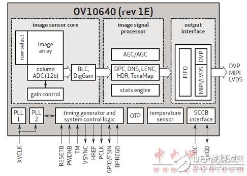
图1.OV10640框图
采用OV10640, DS90UB913A的汽车1.3M照相模块TIDA-00421参考设计
This camera design demonstrates a very small solution size for 1.3 Megapixel automotive cameras. Only a single coax connection is required to provide digital video, power, camera control and diagnostics. Output video format is 10-bit up to 100MHz or 12-bit up to 75MHz.
图2.汽车1.3M照相模块外形图
汽车1.3M照相模块主要特性:
Size optimized design fits on a single PCB 20x20 mm
Power supply optimized for small size and low noise
Diagnostic and Built In Self Test (BIST)
Single Rosenberger Fakracoax connector for digital video, power, control and diagnostics
1.3 Mpixel HDR image sensor OV10640 from OmniVision providing 12bit raw image data
Includes mounting tab for attachment directly to tripod
Power over Coax input can range from 4V to 17V
汽车1.3M照相模块主要应用:
• ADAS Vision Systems
• Surround View Systems
• Rear Camera
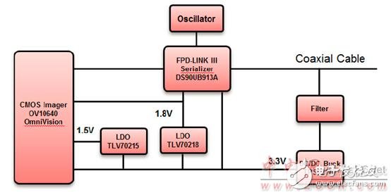
图3.汽车1.3M照相模块参考设计框图
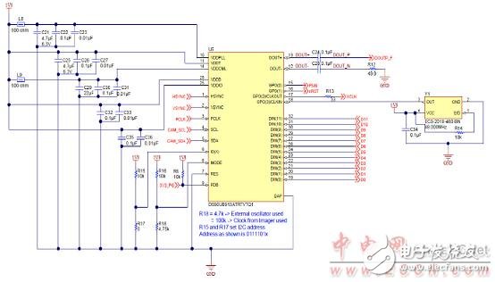
图4.汽车1.3M照相模块参考设计电路图:串行化器
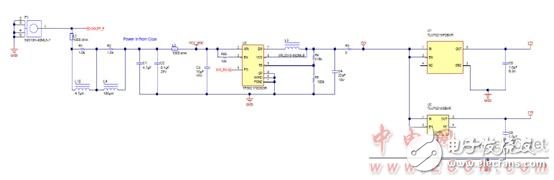
图5.汽车1.3M照相模块参考设计电路图:同轴连接和电源
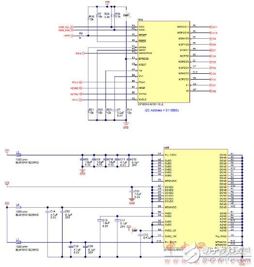
图6.汽车1.3M照相模块参考设计电路图:图像
汽车1.3M照相模块参考设计材料清单:
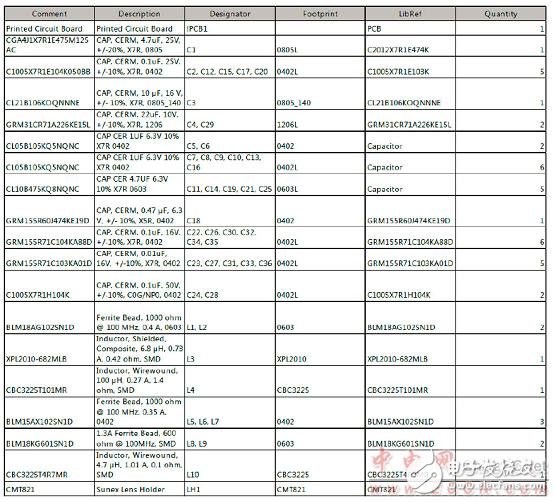
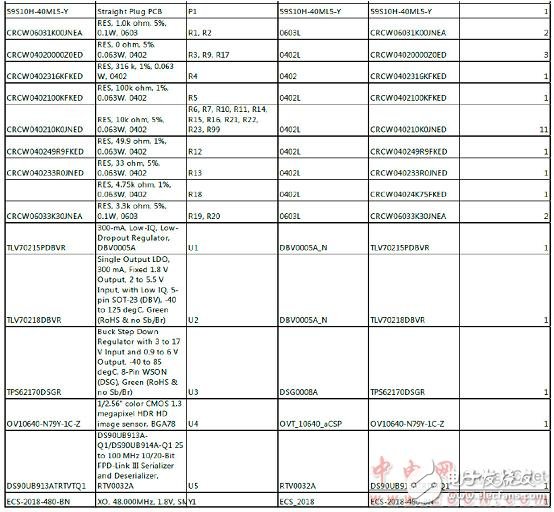
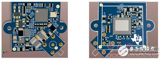
图7.汽车1.3M照相模块参考设计PCB正面和背面外形图
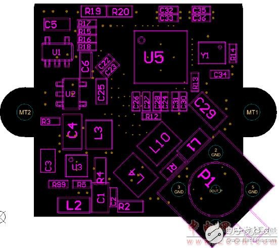
图8.汽车1.3M照相模块参考设计PCB设计图(1)
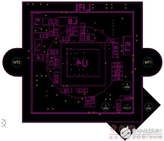
图9.汽车1.3M照相模块参考设计PCB设计图(2)
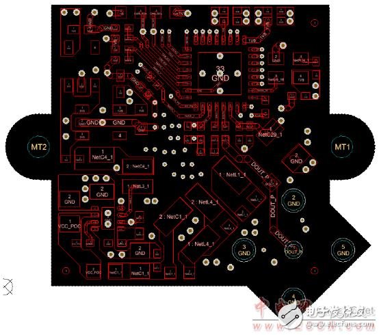
图10.汽车1.3M照相模块参考设计PCB设计图(3)
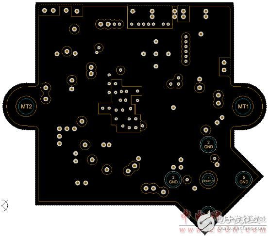
图11.汽车1.3M照相模块参考设计PCB设计图(4)
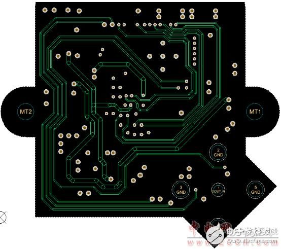
图12.汽车1.3M照相模块参考设计PCB设计图(5)
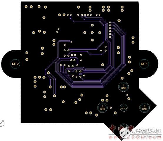
图13.汽车1.3M照相模块参考设计PCB设计图(6)

图14.汽车1.3M照相模块参考设计PCB设计图(7)
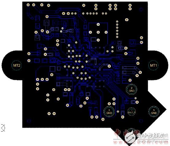
图15.汽车1.3M照相模块参考设计PCB设计图(8)
-
TI TIDA-01179 30W汽车前端电源参考设计2018-04-03 1822
-
迷你STM32照相机(OV7670)设计(转:原理图+源代码)2012-07-26 0
-
自己买的st vl53l0x 激光测距芯片,距离达不到两米,1.3m左右2017-03-07 0
-
基于 STM32+OV7670 的照相机 【原理图、PCB、参考源码】2018-08-22 0
-
LDO为小型照相机提供更高品质的数码照相解决方案2018-08-29 0
-
采用宽输入电压前端的车用摄像头模块设计包括原理图及框图2018-09-12 0
-
集成ISP和DVP输出的汽车ADAS相机集线器包括BOM及层图2018-09-30 0
-
130万像素汽车相机的极小解决方案尺寸包括BOM及层图2018-10-09 0
-
迷你STM32照相机OV76702020-04-01 0
-
迷你STM32照相机(OV76702020-06-10 0
-
PMP10653.1车用摄像头模块设计方案2022-09-15 0
-
大联大世平集团推出基于TI产品的小尺寸电机控制模块参考设计2017-10-17 9778
-
TI TIDA-01425带以太网和CAN的汽车网关参考设计2018-05-19 3498
-
OV7670模块的详细资料合集免费下载2019-04-11 1666
-
为理想ONE汽车装上智能驾驶之“慧眼”2020-06-01 3387
全部0条评论

快来发表一下你的评论吧 !
