

Infineon TLE9879单片汽车三相电机驱动方案
汽车电子
描述
Infineon公司的TLE9879是集成了LIN 2.2与SAEJ2602兼容的LIN收发器和BLDC MOSFET驱动器的微控制器,采用标准的ARM® Cortex™ M3内核,包括了六个全集成的NFET驱动器,适合通过外接六个功率NFET来驱动3相马达,主要用于汽车的燃料泵,HVAC,引擎冷却风扇,水泵和BLDC蚌与风扇.本文介绍了TLE9879主要特性,框图,BLDC马达驱动电路和材料清单,以及评估板TLE9879 EVALKIT,电路图和PCB设计文件图
Microcontroller with LIN and BLDC MOSFET Driver for Automotive Applications
The TLE9879QXA20 is part of the TLE987x product family. The TLE9879QXA20 is a single chip 3-Phase motor driver that integrates the industry standard ARM® Cortex™ M3 core, enabling the implementation of advanced motor control algorithms such as field-oriented control. It includes six fully integrated NFET drivers optimized to drive a 3-Phase motor via six external power NFETs, a charge pump enabling low voltage operation and programmable current along with current slope control for optimized EMC behavior. Its peripheral set includes a current sensor, a successive approximation ADC synchronized with the capture and compare unit for PWM control and 16-bit timers. A LIN transceiver is also integrated to enable communication to the device along with a number of general purpose I/Os. It includes an on-chip linear voltage regulator to supply external loads. It includes an on-chip linear voltage regulator to supply external loads.
It is a highly integrated automotive qualified device enabling cost and space efficient solutions for mechatronic BLDC motor drive applications such as pumps and fans.
TLE9879主要特性:
Six current programmable Drivers with charge pump for N-Channel MOSFET
Integrated LIN transceiver compatible with LIN 2.2 and SAEJ2602
Two Full duplex serial interface (UART) with LIN support
Two Synchronous serial channel (SSC)
On-chip OSC and PLL for clock generation
One high voltage monitoring input with wake up functionality
High speed Operational amplifier for motor current sensing via shunt
Measurement unit:
8-bit ADC module with 10 multiplexed inputs
10-bit ADC module with 8 multiplexed inputs, 5 external Analog inputs
On chip temperature and battery voltage measurement unit
Independent Programmable window watchdog
5V/1.5V Internal supplies
External Supply (VDDEXT): 5V+/-2% @ 20mA
Power saving modes:
MCU slow-down Mode
Sleep Mode
Stop Mode
Cyclic wake-up Sleep Mode
Features of the Microcontroller:
32 bit ARM Cortex M3 Core, up to 24 MHz clock frequency
128 kByte flash memory for code and data
32 kByte Boot ROM memory in code space (used for boot code and IP storage)
6 kByte RAM memory
Harvard architecture
Thumb®-2 Instruction Set and hardware divide and multiplication unit
Four 16-Bit timers
Capture/compare unit for PWM signal generation (CCU6) with 2 x 16-bits timers
General Characteristics:
Operating supply voltage Vs=5.5 to 28V, maximum rating 40V
Extended operating range Vs=3.0 to 28V, MCU / Flash fully functional
ESD performance:
up to 2kV / handling on all pins
4kV @ HV inputs
6kV @ LIN pin
Overvoltage device clamp (load dump ruggedness) up to 40V
Wide operating temperature range: Tj:-40℃ up to 150℃
TLE9879目标应用:
Fuel pump
HVAC blower
Engine cooling fan
Water pumps
BLDC pumps and fans
Sensor-less and sensor-based BLDC motor applications controlled by the Local Interconnect Network (LIN) or PWM
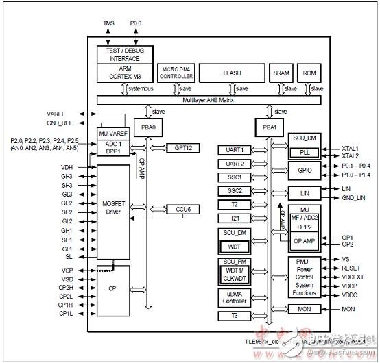
图1。TLE9879框图
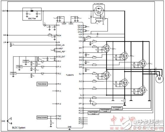
图2。TLE9879简化BLDC驱动器应用电路图
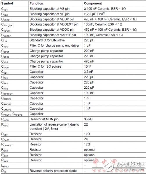
图2中外接元件清单(BOM):
评估板TLE9879 EVALKIT
This board is intended to provide a simple, easy-to-use tool for getting familiar with Infineon’s embedded power IC TLE9879. It contains the TLE9879 and its typical application circuit including three MOSFET half bridges to instantly drive a BLDC motor. The board is ready to connect with car supply or similar and has an implemented Segger for debugging on board.
All relevant chip pins are connected to pin headers at the edge of the board, where signals can be probed or applied directly (see Table 2, Table 3). By different jumper settings LEDs can be put in parallel to several ports and selected functions can be configured (see Table 6). Push button switches allow easy hardware reset and triggering of the MON input. There are intended test points for all six gate driver pins, for measurements at the shunt, VDDC and several ground points on the evaluation board (see Figure 3). For testing analog signals ADC inputs can be varied by the potentiometer on board. Three phases of motor current can be picked off at a terminal block to connect a DC brushless motor.
The evaluation board can be operated by standard laboratory equipment as power supply and LIN communication are working via banana jacks. Debugging and UART are provided via an USB interface combined with onboard Segger J-Link (XMC4200). Bidirectional level shifters ensure that the respective XMC pins are in tristate as long as UART or debugging is not used.
In case the user wants to use another ISP than the onboard Segger the SWD interface can be used. To program the TLE9879 via LIN there is an additional uIO BSL interface (see Table 4).
There is a battery LED that indicates that the board is connected to supply the right way. Otherwise reverse polarity protection secures the board from damage by cross connection.
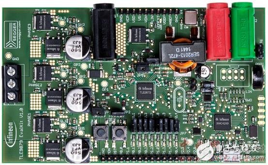
图3.评估板TLE9879 EVALKIT外形图
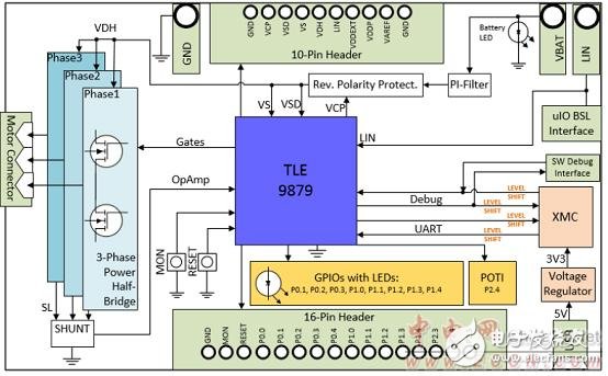
图4.评估板TLE9879 EVALKIT元件布局图
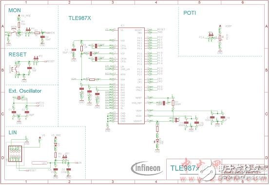
图5.评估板TLE9879 EVALKIT电路图(1)
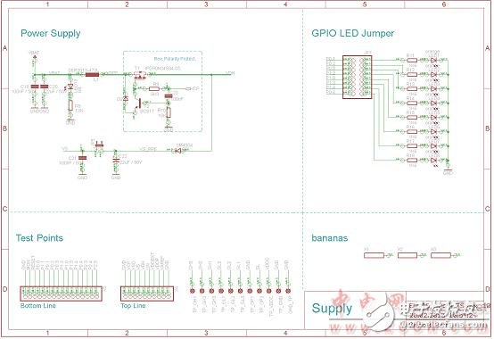
图6.评估板TLE9879 EVALKIT电路图(2)
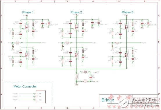
图7.评估板TLE9879 EVALKIT电路图(3)
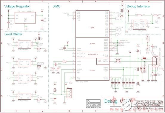
图8.评估板TLE9879 EVALKIT电路图(4)
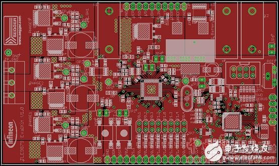
图9.评估板TLE9879 EVALKIT PCB设计师图(1)
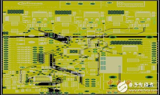
图10.评估板TLE9879 EVALKIT PCB设计师图(2)
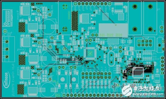
图11.评估板TLE9879 EVALKIT PCB设计师图(3)
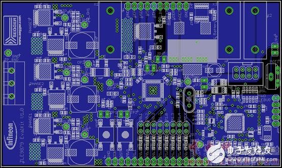
图12.评估板TLE9879 EVALKIT PCB设计师图(4)
-
开发TLE9879芯片的IAR软件的问题求解2024-01-30 0
-
TLE9879和TLE9877的差异是什么?2024-02-01 0
-
TLE9879 EvalKit运行范例TLE9879QXA40_TIMER2_BLINK,P0.2输出(EXF2)没变化是怎么回事?2024-02-02 0
-
TLE9879单电阻方案驱动BLDC如何配置一个周期内采样两次?采样时间如何触发?2024-02-19 0
-
为什么TLE9879 Evaluation Kit提供的原理图是空的?2024-02-20 0
-
TLE9879 Evakit开发板输出异常怎么解决?2024-03-04 0
-
tle9879系列的pwm占空比是多少?2024-03-05 0
-
TLE9879 PWM的最大频率到底是多少?2024-03-05 0
-
TLE9879 demo无法下载2018-12-17 0
-
Infineon TLE9879QXA40 BLDC Arduino马达控制方案2019-08-11 0
-
Infineon TLE9879单片汽车3相马达驱动方案2018-05-16 7069
-
TLE9879汽车三相马达驱动解决方案2019-04-05 5886
-
TLE9879板FOC无传感器的工程文件免费下载2021-02-02 764
-
英飞凌TLE9879无刷电机原厂英文资料2022-06-20 367
-
英飞凌TLE9879资料2022-06-20 513
全部0条评论

快来发表一下你的评论吧 !
