

MAX14483优势和特性/应用电路_评估板MAX14483 EVK电路图及PCB设计图
电子说
描述
Maxim公司的MAX14483是六路3.75kVRMS数字电隔离器,采用公司的专有工艺技术,最佳用于SPI接口,在SDI,SDO和SCLK通路有非常低的传输时延,典型时延10ns,时钟高达100MHz,数据速率高达200Mbps,脉宽失真小于2ns,典型抖动250ps, 主要用在可编逻辑控制器(PLC),工业自动化,过程自动化,建筑物自动化,机器人和通用SPI总线隔离。本文介绍了MAX14483优势和特性,功能框图,多种应用电路,以及评估板MAX14483 EVK主要特性,电路图,材料清单和PCB设计图。
The MAX14483 is a 6-channel, 3.75kVRMS digital galvanic isolator using Maxim’s proprietary process technology. The six signal channels are individually optimized for SPI applications and include very low propagation delay on the SDI, SDO, and SCLK channels. The SDO channel’s tri-state control is enabled by the CS input as well as a second enable control input pin (SDOEN), allowing a single MAX14483 to isolate multiple SPI devices. To simplify system design, an open-drain FAULT output can be wire ORed with error outputs from other devices. In addition, an auxiliary channel (AUX) is available for passing timing or control signals from the master side to the slave side and power monitors (SAA, SBA) are provided for both power domains to signal if the opposite side of the isolator is ready for operation. Independent 1.71V to 5.5V supplies on each side of the isolator also make the device suitable for use as a level translator.
The MAX14483 has an isolation rating of 3.75kVRMS for 60 seconds and is available in a 20-pin SSOP package with 5.5mm of creepage and clearance. The package material has a minimum comparative tracking index (CTI) of 400V, which gives it a group 2 rating in creepage tables.The MAX14483 is rated for operation at ambient temperatures of -40℃ to +125℃。
MAX14483优势和特性:
Saves Space and Components6 Isolated Channels in a 20-SSOP Package
Low Propagation Delay on SCLK, SDI, and SDOUp to 100MHz Clock, 200Mbps Data Rate
10ns Typical Propagation Delay
2ns Maximum Pulse Width Distortion
250ps Typical Peak Jitter
Robust Galvanic Isolation of Digital SignalsWithstands 3.75kVRMS for 60s (VISO)
Continuously Withstands 450VRMS (VIOWM)
Withstands ±10kV Surge between GNDA and GNDB with 1.2/50μs Waveform
High CMTI (50kV/μs, Typical)
Flexible System DesignWide 1.71V to 5.5V Voltage Range on Each Side
SDOEN Control Pin for Sharing Isolators
Open-Drain FAULT Channel for Shared Interrupt on Master Side
Auxiliary Channel for Timing or Control
Low Power Consumption1.53mW per Channel at SCLK = 10MHz withVDD = 3.3V
0.77mW per Channel at SCLK = 10MHz withVDD = 1.8V
MAX14483应用:
Programmable Logic Controllers
Industrial Automation
Process Automation
Building Automation
Robotics
General SPI-bus Isolation
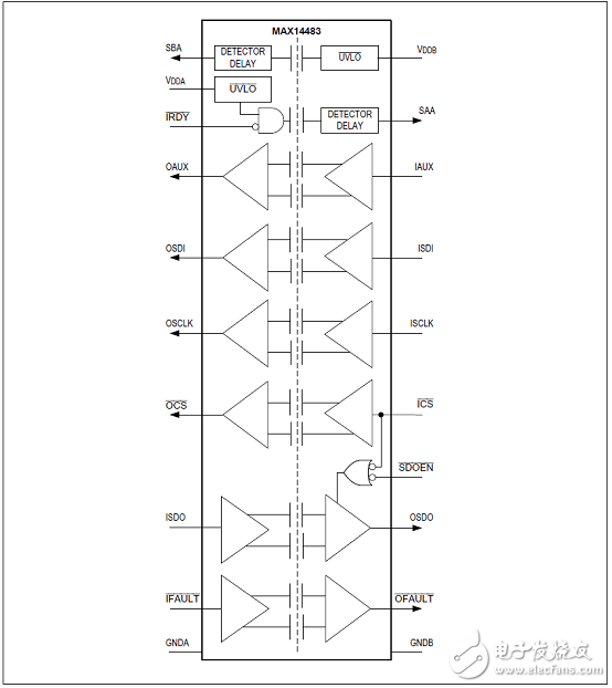
图1.MAX14483功能框图
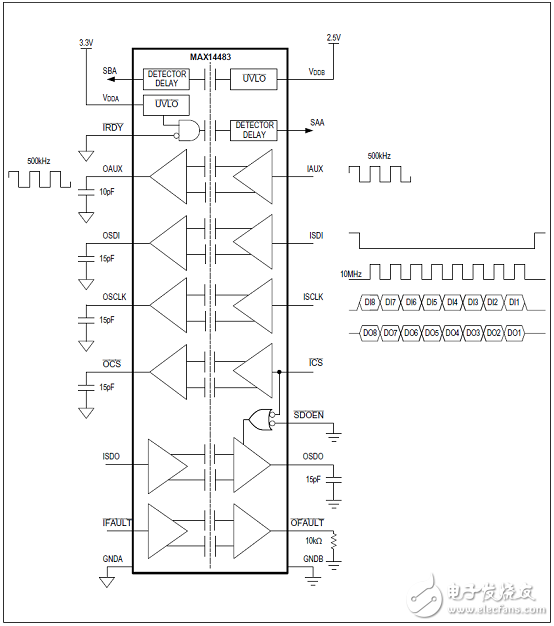
图2.MAX14483电流计算案例应用电路图
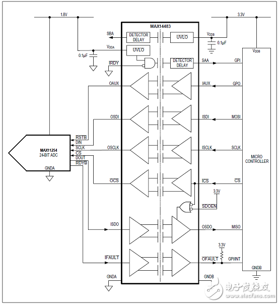
图3.MAX14483隔离的SPI接口电路
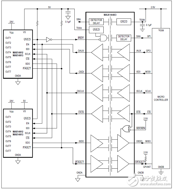
图4.MAX14483隔离的SPI菊花链,16个数字输出
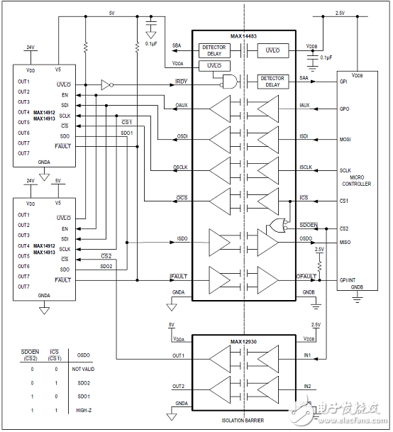
图5.MAX14483隔离的单独从SPI总线,16个数字输出
评估板MAX14483 EVK
The MAX14483 evaluation kit (EV kit) provides a proven design to evaluate the MAX14483, 6-channel, 3.75kVRMS, SPI digital isolator. The EV kit allows easy access to all six channels through either SMA connectors or test points. On-board LEDs on the ready signals (SAA and SBA) and FAULT output directly indicate the signals’status.
The EV kit should be powered from two independent isolated power supplies with nominal output voltage in range from 1.71V to 5.5V. For evaluating the electrical parameters of the device without any isolation between the two sides, a single power supply can also be used.
The MAX14483EVKIT# comes populated with the MAX14483AAP+ installed in a 20-pin SSOP package with 5.5mm of creepage and clearance.
评估板MAX14483 EVK主要特性:
Six Unidirectional Channels with Different Channel Direction Configuration and Data Speed (Up to 200Mbps)
On-Board LEDs Indication of Device Ready for Communication
SMA Connectors for Easy Connection to External Equipment
Wide Power Supply Voltage Range from 1.71V to 5.5V
Guaranteed Up to 3.75kVRMS Isolation for the 20-pin SSOP Package for 60s
-40℃ to +125℃ Temperature Range
Proven PCB Layout
Fully Assembled and Tested
图6.评估板MAX14483 EVK外形图
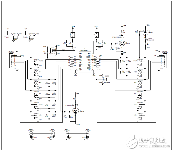
图7.评估板MAX14483 EVK电路图
评估板MAX14483 EVK材料清单:
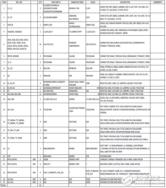
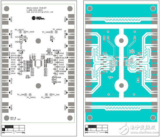
图8.评估板MAX14483 EVK PCB设计图:左:顶层丝印;右:顶层
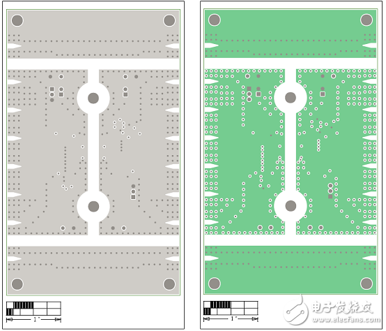
图9.评估板MAX14483 EVK PCB设计图:左:层2 GND;右:层3 PWR
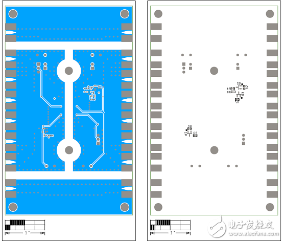
图10.评估板MAX14483 EVK PCB设计图:左:底层;右:底层丝印
-
PCB电路图设计图教程jf_76415565 2022-09-03
-
max232应用电路原理图2008-10-21 0
-
MAX16804高亮度LED驱动器评估板电路原理图2011-01-02 0
-
MAX1840, MAX1841典型应用电路图2011-08-06 0
-
max232通讯电路图2012-11-07 0
-
请问有人能根据我的描述意图画出大致的电路图或者PCB设计图吗?2018-01-12 0
-
基于Maxim MAX13335E/MAX13336E的汽车高保真立体声音频输入方案2018-06-16 3816
-
Maxim MAX30001超低功耗生物电势和阻抗AFE的解决方案详解2018-06-18 7927
-
一文详解IDP2303的主要特性/应用电路图及PCB设计图2018-06-16 18981
-
Maxim MAX22444-6快速低功耗四路数字电流隔离器解决方案2018-07-22 3821
-
Maxim MAX77640/MAX77641超低功耗PMIC解决方案2019-04-05 5031
-
MAX40056主要特性以及应用电路2019-04-05 5383
-
MAX28200优势特性以及基本应用电路2019-04-05 1436
-
MAX86150的优势特性以及典型应用电路图2019-04-05 5280
-
MAX14483AAP+ 数字隔离器2023-02-03 22
全部0条评论

快来发表一下你的评论吧 !
