

详解ucc28C43-Q1PWM控制方案(特性,指标,框图,电路图)
控制/MCU
描述
TI公司的ucc28C43-Q1是 BiCMOS高性能低功耗电流模式PWM控制器,满足AEC-Q100规范,工作温度-40⁰C到125⁰C,HBM分类为Level 2: ±2 kV, CDM分类Level C4B: 750 V,工作频率1MHz,峰值输出电流±1-A,主要用在汽车电源,混合和电动汽车,开关电源,DC/DC转换器,板安装电源模块.本文介绍了UCC28C43-Q1主要特性,功能框图, 汽车应用电路图,以及汽车应用40V-1kV输入反激参考设计TIDA-01505主要特性和系统指标,框图,电路图和材料清单.
The UCC28C4x-Q1 family devices are high performance current-mode PWM controllers. They are enhanced BiCMOS versions with pin-for-pin compatibility to the industry standard UC28C4x family PWM controllers.
Providing necessary features to control fixed frequency, peak current mode power supplies, this family offers several performance advantages. These devices offer high frequency operation up to 1 MHz with low start up and operating currents, thus minimizing start up loss and low operating power consumption for improved efficiency. The devices
also feature a fast current sense to output delay time of 35 ns, and a ±1-A peak output current capability with improved rise and fall times for driving large external MOSFETs directly.
The UCC28C4x-Q1 family is offered in the 8-pin SOIC (D) package.
UCC28C43-Q1主要特性:
1• AEC-Q100 Qualified with the Following Results:
– Device Temperature Grade 1:-40⁰C to 125⁰C
– Device HBM Classification Level 2: ±2 kV
– Device CDM Classification Level C4B: 750 V
• 1-MHz Operation
• 50-μA Standby Current, 100-μA Maximum
• Low Operating Current of 2.3 mA at 52 kHz
• Fast 35-ns Cycle-by-Cycle Over-Current Limiting
• ±1-A Peak Output Current
• Rail-to-Rail Output Swings With 25-ns Rise and 20-ns Fall Times
• ±1% Initial Trimmed 2.5-V Error Amplifier Reference
• Trimmed Oscillator Discharge Current
• New Undervoltage Lockout Versions
• Create a Custom Design Using the UCC28C4x-Q1 With the WEBENCH® Power Designer
UCC28C43-Q1应用:
• Automotive Power Supplies
• Hybrid and Electric Vehicles in Automotive
• Switch Mode Power Supplies
• DC-to-DC Converters
• Board Mount Power Modules
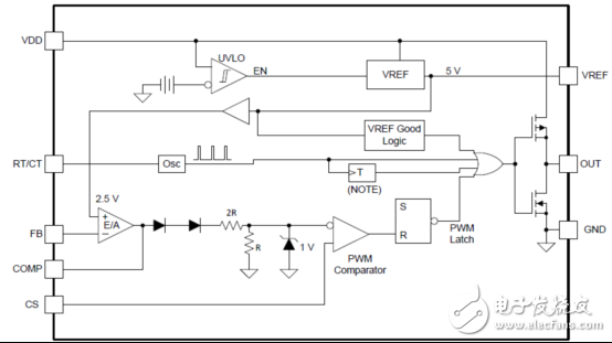
图1. UCC28C43-Q1功能框图
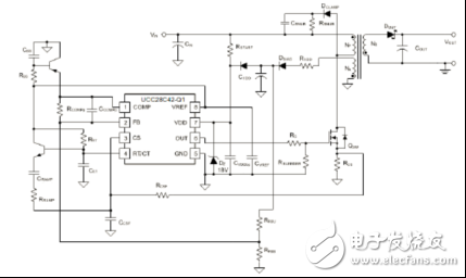
图2. UCC28C43-Q1汽车应用电路图
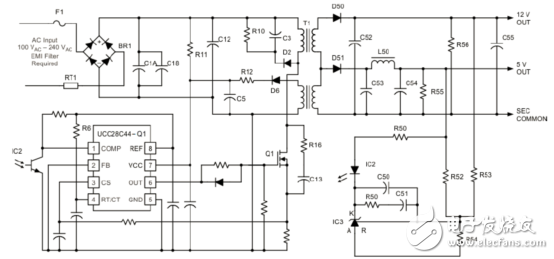
图3. UCC28C43-Q1典型离线应用电路图
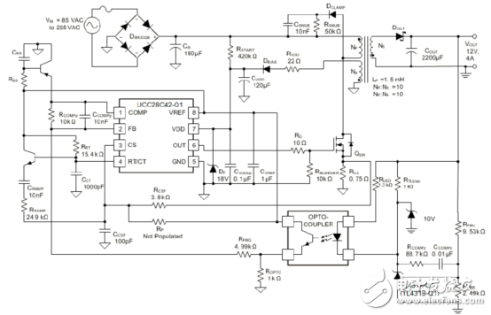
图4. UCC28C43-Q1典型应用电路图
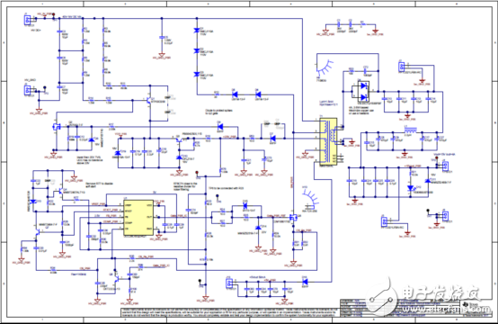
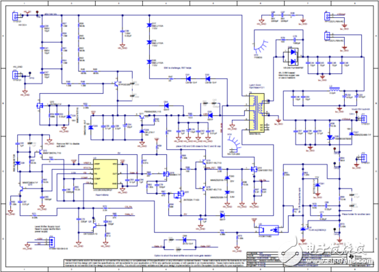
汽车应用40V-1kV输入反激参考设计TIDA-01505
This power supply reference design for automotive auxiliary circuits generates a 15-V, 4-A output from a wide input range of 40 V to 1 kV and up to a 1.2-kV transient. The design fits ideally into an 800-V batterydriven hybrid-electric vehicle (HEV) or electric vehicle (EV) traction inverter system. The 40-V minimum input voltage supports the functional safety test for the regenerative braking from the traction motor. This reference design implements a silicon carbide (SiC) MOSFET with high blocking voltage and low gate charge to reduce switching losses. A non-isolated level shifter enables driving the SiC MOSFET from the Si MOSFET driver embedded in the flyback controller.
The board includes two flyback converter variants:
primary-side regulation (PSR) and optocoupler feedback to make comparisons and address different needs. The transformer design meets qualifications for Automotive AEC-Q200 Grade 1 with reinforced isolation.
This reference design is a 60-W power supply which enables an ultra-wide input range from a 40-V (minimum) to 1-kV (maximum) DC voltage targeted for use in 800-V battery systems. A primary feature of this design is that the converter can power up at the 40-V minimum input voltage, which allows support for the system safety test during the regenerative braking for traction inverters. This design is an auxiliary power supply solution that generates a 15-V output for the traction inverter subsystems. The design also
implements reinforced isolation for safety enhancement. The single-ended, flyback topology has been chosen due to its low cost, high isolation rating, and design simplicity. Moreover, the design includes two onboard converter variants, with optocoupler and primary side regulation (PSR) for performance comparisons.
Carefully consider the following criteria to fulfill the design requirements:
• Voltage blocking capability of the switching device –
Because of the high voltage, the Si MOSFET, which has a lower design margin for blocking voltage and high channel resistance, is not suitable. The design requires use of an SiC MOSFET with a higher blocking capability.
• Pulse-width modulated (PWM) switching duty cycle –
Support for such an ultra-wide input voltage range requires a controller that is able to operate within the corresponding, wide PWM duty-cycle range.
• Active start-up circuit –
The traditional, resistive start-up circuit causes high quiescent losses at high input voltage. This design implements an active start-up circuit for reduced leakage current.
• Noise coupling –
The high-voltage input and fast switching of the SiC MOSFET leads to high dv/dt switching nodes, which generates a large amount of noise and antenna loops. The essential switching nodes must be kept small and away from quiet areas to reduce the noise coupling.
• Safety clearance –
The distance between the high-voltage area at the primary side and low-voltage area at the secondary side must have enough clearance to comply with safety requirements. Reinforced isolations are normally imposed according to automotive safety requirements. The ground of the low-voltage side may be connected to a 12-V battery or vehicle chassis, which is touchable by the human body.
• Printed-circuit board (PCB) clearance and high-voltage components selection –
The PCB clearance must be carefully designed to avoid electrical breakdown failure. Carefully select components that tolerate high voltages to properly handle the high-voltage stress.
This reference design is capable of powering up from a 40-V minimum input voltage for the purpose of enabling engineers to work safely and allow them to test the regenerative braking mechanism.
Regenerative braking utilizes the same insulated-gate bipolar transistor (IGBT)-based traction inverter to force the power flow in the reverse direction from the motor and send the power back to the battery. The IGBTs are controlled in a different algorithm to regulate the DC output from AC. Regenerative braking technology funnels the energy created by the braking process back into the system in the form of charging the battery for further use. Typically, in a regenerative braking system, the energy loss from the braking process transfers to the generator from the rotating axel before transferring to the battery, thus saving energy.
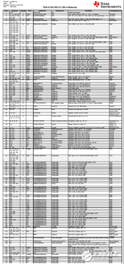
参考设计TIDA-01505主要特性:
• 40-V to 1-kV input, 15-V Output Flyback Auxiliary Power Supply With Output Power up to 60 W
• Regulated 15 V With Active Start-Up Circuit for Reduced Standby Power
• Extendable to Higher Voltage and Higher Power Range to Utilize High-Voltage Capability of SiC MOSFET
• Automotive Grade 1 Qualified Transformer With Reinforced Isolation (Qualified With 5.7-kV High- Pot Test)
• Two Converter Variants With PSR and Optocoupler Feedback Included on Board
• Constant Switching Frequency Type of Controller With Maximum Switching Frequency of 1 MHz and Duty Cycle Range From 0% to 96%
参考设计TIDA-01505应用:
• HEV/EV Traction Inverter
• HEV/EV On Board Charger
• Electronic Control Units
• HEV/EV DC/DC Converters
图5. 参考设计TIDA-01505外形图
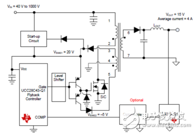
图6. 参考设计TIDA-01505框图
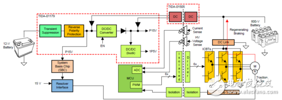
图7. 800V电池驱动逆变系统和实现TIDA-01505的框图
主要系统指标:
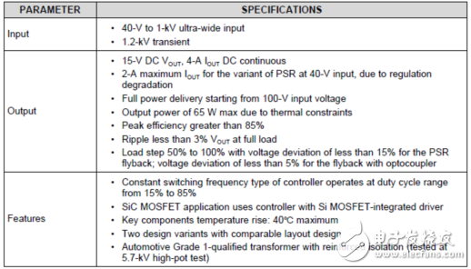
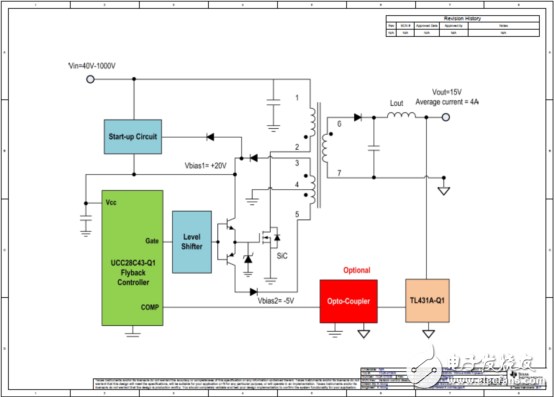
图6. 参考设计TIDA-01505框图
-
PWM控制器UCC38083资料推荐2021-03-26 0
-
长虹43PT28B电路图2008-10-13 0
-
UCC28950 600W高性能电源系统解决方案2011-09-08 0
-
PWM控制器UCC28085资料推荐2021-03-26 0
-
LMP91050有什么主要指标和特性?2021-04-08 0
-
使用UCC5870-Q1和UCC5871-Q1增加HEV/EV牵引逆变器的效率2022-11-03 0
-
长虹43PT28A电路图纸2008-10-13 890
-
长虹43PT28B电视机电路图2008-10-13 913
-
基于UCC28070设计的300W PFC高效电源方案2010-08-20 4614
-
一文详解UCC28780主要特性_功能框图及典型应用电路图2018-06-16 20276
-
UCC28C43-EP BiCMOS 低功耗电流模式 PWM 控制器2018-11-02 400
-
UCC28C43 BiCMOS 低功率电流模式 PWM 控制器2018-11-02 1227
-
UCC28C43-Q1 UCC28C4x-Q1 BICMOS 低功耗电流模式 PWM 控制器2018-11-02 636
-
UCC28C43QDRQ1开关电源简介2022-09-16 2395
-
UCC28C43国产替代料AP8262C电流模式pwm芯片规格书2023-11-28 227
全部0条评论

快来发表一下你的评论吧 !
